Products

System simulation solution
Chip simulation solution
System simulation solution
SI-Designer allows designers to intuitively find problems and defects in the design, adjust them timely, and thereby effectively solving problems of high-speed signal integrity.
Chip simulation solution
TJPICE is the industry’s leading SPICE simulator for general circuit simulation with golden accuracy, which can perform simulation and verification of chip model library and IO circuit design.


Application Case
Case of Parallel Interface Signal Integrity Analysis Realized in SIDesigner
Signal Integrity Simulation Platform
Preface
As parallel interfaces such as DDR and EMMC are used more and more widely in the fields of consumer electronics and high-end server products, data rates are getting the highest than ever. Due to the strong mutual interference among signals when parallel interfaces are switched synchronously, jitter and power supply noise will cause a large system timing loss. Once this problem is found after the completion of the design, the redesign will result in a massive cost loss. Therefore, it is important for engineers to analyze the signal integrity and power integrity of the parallel interface before and during the design to ensure that the rate meets the specifications.
Signal integrity analysis is generally divided into two steps: physical modeling by EM solver and system timing circuit analysis by the SPICE tool. In the pre-layout stage, due to the lack of specific layout physical design, a similar PCB or the package design model is evaluated with the transmission line model and the via model according to the actual situations, so there often exists a certain expectation about the system result in the initial stage of the design. As a circuit-level simulation platform for signal integrity and power integrity, SIDesigner can perform system-level signal integrity analysis, power integrity analysis, or system timing performance evaluation in the pre-layout phase when the physical model of PCB and Package is already available. This case introduces the signal integrity analysis of the parallel interface in the pre-layout stage based on the SIDesigner simulation platform, involving the IBIS model, S-parameter model, and transmission line model.
Preparation before Simulation
Before the simulation and evaluation start, it is necessary to amply prepare the full picture of the object to be simulated and the content to be evaluated, the so-called garbage-in garbage-out. In this case, LPDDR3 is used as an example and one byte of it is to be evaluated for its signal integrity. The preparation is as follows:
1)DDR interface rate: Take 1Gbps as an example for simplicity.
2)DDR TX/RX IO model: Take writing as an example, TX is the controller, the IP provider of the control chip needs to provide the IO model, RX is DRAM, and the DRAM manufacturer needs to provide the corresponding IO model.
3)Channel model: The package model is provided by DRAM and controller manufacturers. Since the PCB has not been designed, it is replaced by a transmission line model close to the design one.
4)Power supply model: In the pre-layout evaluating stage, an ideal power supply is configured without considering the influence of power supply noise.
After the above preparation is ready, the system-level signal integrity simulation work in SIDesigner is to start.
The detailed steps of signal integrity simulation for parallel interface in SIDesigner
The final circuit structure diagram of this case is as follows, and the building process will be introduced step by step.
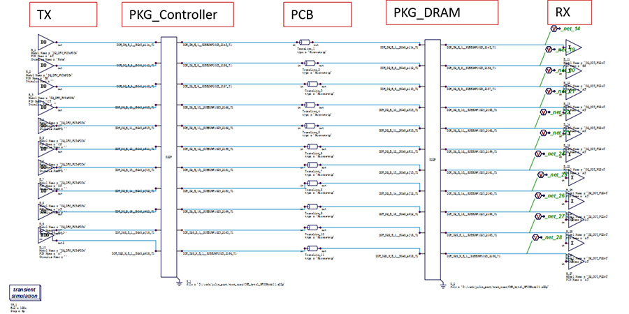
Figure 1. The Final Circuit Structure Diagram
Step 1: Create a Project
Step 1:
In SIDesinger, a new Solution needs to be created firstly, then create a Project, and name it. Under Project, specific circuit schematics can be created.
Usually after the creation is completed, the path where the S parameter model and the IO IBIS model used for simulation are located is set, so that they can be quickly obtained during subsequent settings
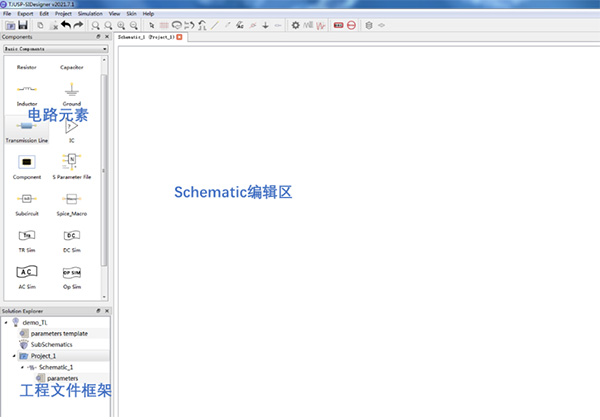
Figure 2. Create a New Project
Step 2: Instantiate the IO Model
Place the IO buffer model and instantiate it: Import the IBIS file, select the corresponding component, and then select the pin and the corresponding IO model to complete the IO instantiation one by one. Note that the responding output and input models need to be set for the sender and receiver. The below figure 3 shows the Output model, and the driver is set as 34ohm.
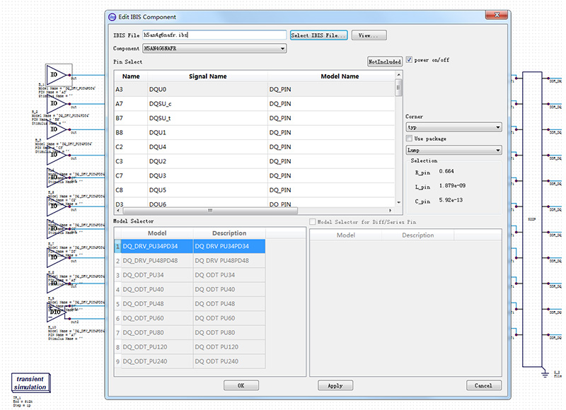
Figure 3. The IO Instantiation
Step 3: Set Stimulus
After the instantiation of the IO model is completed, the stimulus can be set for the IO at the sender. SIDesigner supports different types of stimulus setting, including PRBS, PWL, Pulse, PAT, and various file-based input formats. In DDR interface simulation, DQ signal is usually stimulated by PRBS, and DQS signal is stimulated by PULSE.
It should be noted that for the DDR interface, there is a response delay between DQ and DQS according to SPEC requirements, which must be taken into consideration when setting the simulation stimulus.
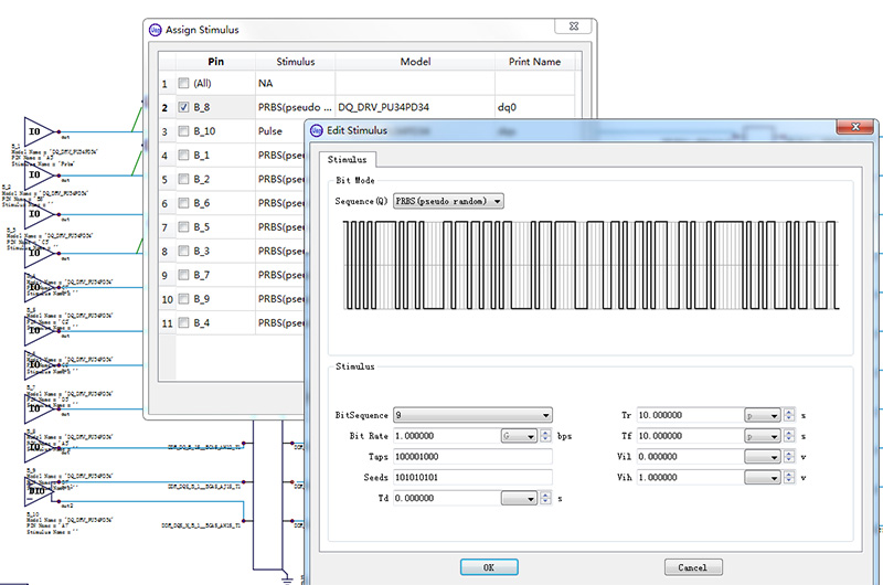
Figure 4. The IO Stimulus Setting
Step 4: Create a Channel Model
In the signal integrity simulation, Channel is generally composed of S-parameters or responding wide-band circuit models. In the pre-layout stage, there are also transmission lines and via models as supplements.
This example is a combination of S-parameters and transmission lines.

Figure 5. S Parameters Importing
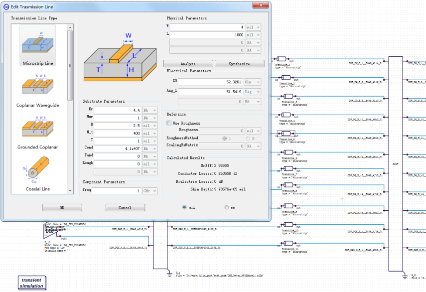
Figure 6. The Transmission Line Setting
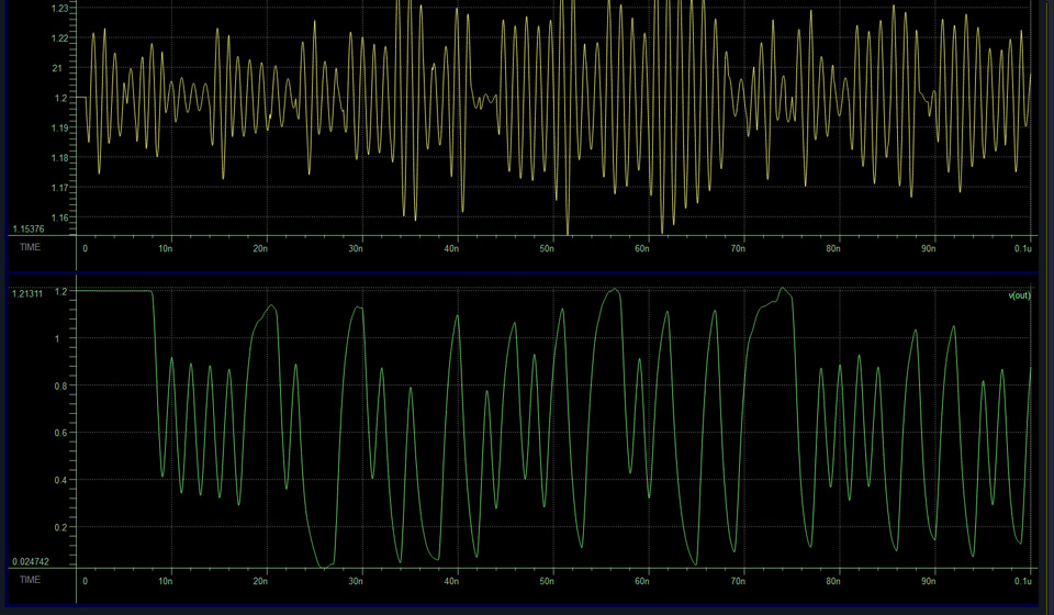
Step 5: Simulation Settings
After the system circuit is built, the waveform/eye diagram observation points and transient simulation control are added, as shown in the following figure:
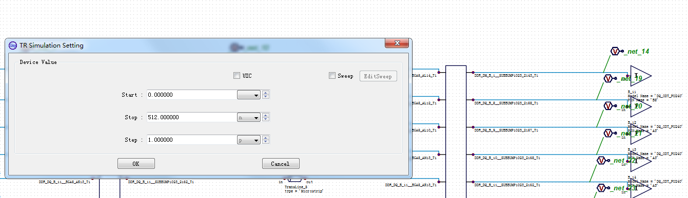
Figure 7. Time Domain Setting
The stimulating time is measured by the code length *UI, and the observation point generally takes the stimulus point and the input point of the receiver as the mandatory points.
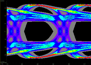
Step 6: Waveform Viewing and Post-processing
Once the simulation is over, the built-in waveform processor of SIDesigner automatically allows the import of the generated waveform, and the user can perform post-processing and measurement towards the simulation result.

Figure 8. The Simulation Result and Post-Processing
Summary
This article uses a simple DDR simulating case to introduce how to complete the signal integrity analysis of the parallel interface in SIDesigner. As a general circuit simulation platform mainly for signal integrity analysis, SIDesigner can complete all SI/PI related work except 3D EM modeling. Users can conveniently perform various what-if analyses in this platform to explore the optimization of design.
Simulate a Better Future

Scan The QR Code To Follow Us