












Why Is Full-Board SI Verification Prone to Missing Checks?
-
 2026.09.18
Before a PCB is sent for fabrication, SI engineers typically bring the stackup, actual routing, vias, and device models into post-layout simulation to check whether signal waveforms and key performance metrics meet the design requirements.
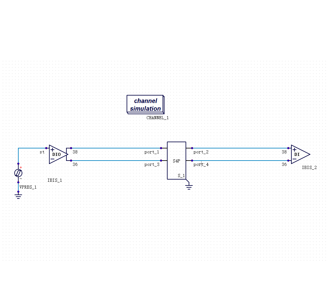
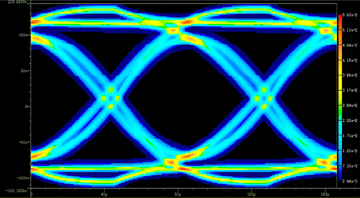
For a single net, the workflow is relatively straightforward: select the net, configure the driver and receiver models, define the excitation and probe points, run the simulation, and then check the waveform, rise/fall time, or eye diagram.
When the verification scope expands to the entire PCB, however, the task changes significantly. The same board may contain DDR data, clock, address, and control signals, as well as conventional single-ended signals, differential signals, and signals crossing between boards. The fact that an individual net can be successfully simulated does not mean that full-board verification has been completed.
An even harder-to-detect situation occurs when a net is renamed during a design iteration but the original verification list is not updated accordingly. Other nets can still generate results normally, while the omitted net does not trigger any error.
Full-board SI verification therefore needs to answer three questions simultaneously:
Are all critical nets covered? Are the simulation conditions consistent? Can the results be reviewed against the same criteria?

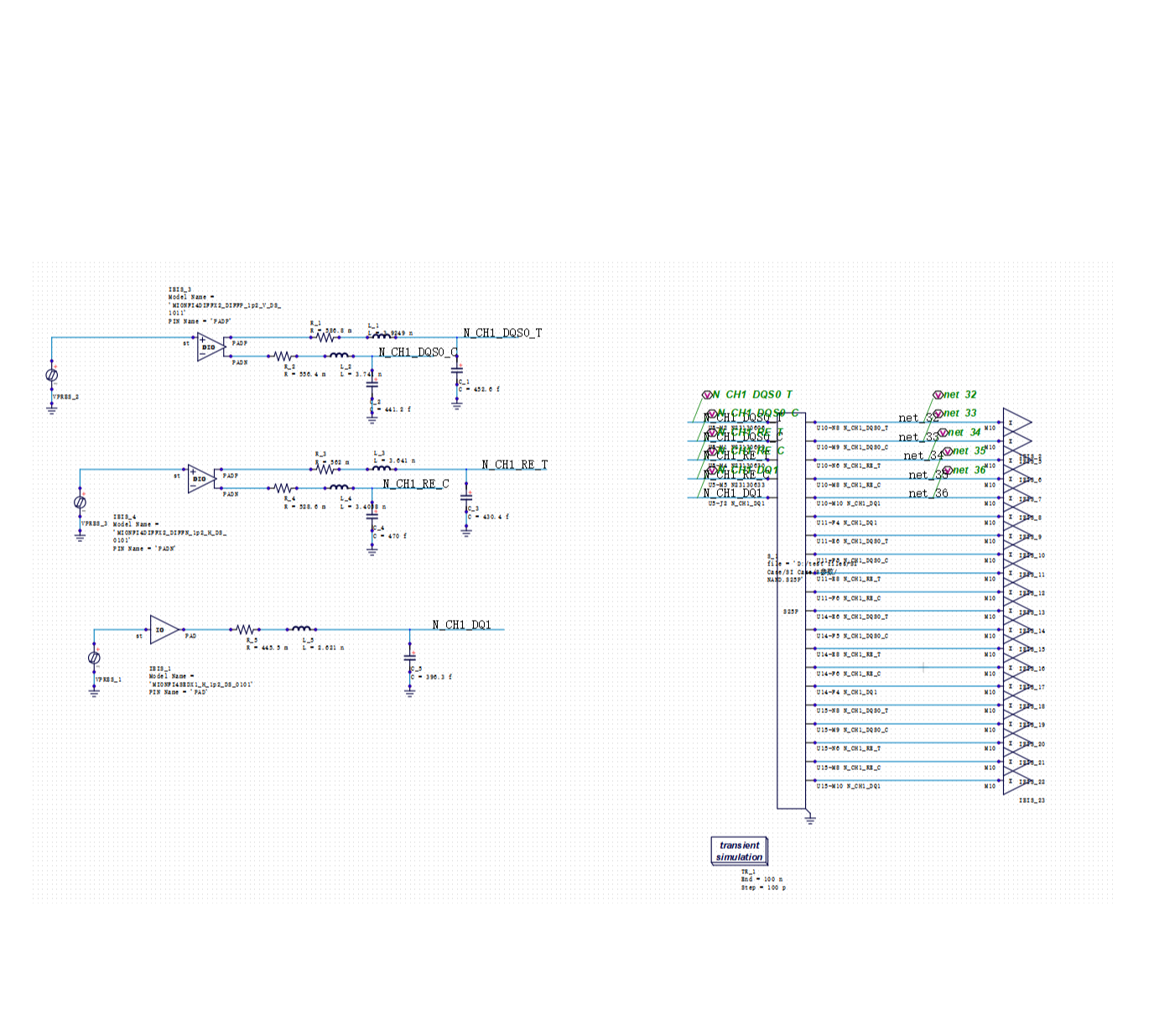
From a single link to a full-board collection of nets. As the verification scope expands, the task evolves from running one simulation to managing net coverage and simulation conditions.
Scale: Both Nets and Operating Conditions Increase
Full-board post-layout simulation increases not only the number of nets, but also the coupling relationships between nets and the operating-condition combinations associated with each net.
For high-density interfaces such as DDR data and address signals, the result of an aggressor/victim net can be affected by neighboring signals. To evaluate near-end crosstalk, far-end crosstalk, and their impact on waveforms, eye diagrams, and timing margins, coupled nets often need to be simulated simultaneously under the same operating conditions.
The verification target therefore changes from a single link to a collection of coupled nets.
The same group of nets may also need to be checked under different process corners, RLC parameters, or device models. For multi-board systems, the mapping between connector pins and S-parameter ports also needs to be verified.
As both the number of nets and operating conditions increase, the verification process needs to consistently manage six categories of information:
Critical nets to be verified;
Models, excitations, and probe points;
Coupled nets and crosstalk conditions;
Variables that need to be swept;
Measurement metrics and pass/fail criteria;
Risk items that need to be returned to the design team for further action.
When this information is scattered across operation records, temporary spreadsheets, waveform windows, and multiple report versions, it becomes difficult for the team to determine whether the entire board has been verified using consistent criteria.
Missing Items: Unselected Nets Do Not Trigger Errors
Net-by-net post-layout simulation relies on engineers maintaining a net list and confirming the driver direction, probe points, and signal grouping for each item.
If components are replaced, net names are modified, or connectivity is changed during the design process, the verification list also needs to be updated accordingly.
An omitted net does not affect the execution of other simulations.
Nets that have already been selected can still generate waveforms and reports normally, while a net that has not been included in the verification scope does not actively generate an alert.
Therefore, the first question in full-board verification is not whether an individual waveform is correct, but whether all critical nets have been completely covered.
Configuration: Repetitive Operations Make Consistent Conditions Difficult to Maintain
Even when no nets are missing, it does not necessarily mean that the verification conditions are consistent.
Different signals within the same interface may use different driver or receiver models. Probe points may be located at package pins for some signals and at chip-side locations for others. Process corners may also be mixed between typical, fast, and slow settings.
RLC component values and connection states, excitation frequency, pattern length, simulation time, and time step can likewise vary during repeated configuration.
These differences directly affect result comparison.
When a waveform changes, engineers need to determine whether the change comes from the actual routing or from differences in the model, excitation, or probe location.
If the configuration is not consistently recorded, the results become difficult to reproduce and review.
Evaluation: Generating Waveforms Does Not Mean Verification Is Complete
Different types of signals require different metrics.
For conventional signals, engineers may focus on peak-to-peak voltage, rise time, and fall time. For DDR data lines, eye height and eye width also need to be checked.
Each result needs to be compared against the corresponding Spec, or engineering acceptance criterion.
The evaluation threshold may come from an interface specification or from project-level requirements. It should not be determined temporarily while reviewing the waveform.
When the number of nets is relatively small, engineers can inspect waveforms one by one and then organize screenshots into a report.
As the verification scope expands, however, manual evaluation introduces new problems:
Is the same measurement method being used for the same metric?
Are the correct thresholds configured for each net?
Can an abnormal item in the report be traced back to the original net and topology?
After a design modification, can the relevant results be rerun under the original conditions and the report updated accordingly?
If this information depends on individual memory, the report may only summarize the results without forming a traceable verification record.

Process gaps in full-board verification: missing nets, configuration differences, scattered evaluation criteria, and difficulty tracing results back to the original topology.
Full-Board Verification Requires a Test Plan
In a rigorous full-board verification process, the starting point is usually not the temporary selection of nets after opening the simulator, but a predefined Test Plan.
The Test Plan should lock down the net set to be verified, model versions, excitation and probe locations, process corners, and crosstalk conditions.
It should also predefine the measurement metrics and acceptance thresholds for different types of signals.
Single-net simulation answers one question:
How does this link perform under the current conditions?
Full-board verification needs to go further by confirming:
Net coverage;
Configuration consistency;
Unified measurement;
Anomaly traceability;
Re-verification after design changes.
As the number of critical nets continues to increase, breaking full-board verification into multiple independent single-net operations can leave gaps in the workflow.
Engineering experience can identify some problems, but it cannot replace a stable and reviewable verification record.
Full-board PCB SI post-layout verification needs to use the Test Plan as its baseline, bringing the board layout, nets, models, operating conditions, measurement criteria, and reports into the same workflow.
This makes it clear which verification items have been completed, which results present risks, and where the design team needs to continue making changes.
When the design changes, the team can also use the same baseline to identify affected verification items and rerun the simulations under the original conditions before updating the report.
In the next article, we will introduce a batch transient verification workflow for critical nets across an entire PCB, and explain how to move from the board layout to a report that is both determinable and traceable.


Recommended
-
 The Two Structural Barriers in Power Electronics Simulation: Model Portability and Signoff Accuracy
 2026.07.02
 -
 Optimizing DDR Signal Integrity: Using DFQ Sensitivity Analysis (S1/ST) to Identify High-Leverage Design Variables
2026.06.10
Optimizing DDR Signal Integrity: Using DFQ Sensitivity Analysis (S1/ST) to Identify High-Leverage Design Variables
2026.06.10 -
 Efficiency Bottleneck in DDR5 Multi-Corner Timing Verification: PDA Analysis Methods
2026.05.27
Efficiency Bottleneck in DDR5 Multi-Corner Timing Verification: PDA Analysis Methods
2026.05.27 -
 The Mass Production Yield Trap After DDR5 SI Sign-off: Using DFQ to Predict Defect Rates Early
2026.05.07
The Mass Production Yield Trap After DDR5 SI Sign-off: Using DFQ to Predict Defect Rates Early
2026.05.07