











China's Domestic EDA Enters the “Deep Water”: How Is Julin Technology Opening a Path Through SI/PI Simulation?
-
 2026.09.08
The following article is sourced from Zhang Guobin, author at Electronic Innovation Network.
China's domestic EDA industry is entering an increasingly practical stage.
In the past, discussions about domestic EDA were more focused on questions such as: “Do we have the tools?” and “Can they replace overseas alternatives?” Today, however, the real question facing domestic EDA vendors has become: Why would customers be willing to entrust their real projects to you?
This is particularly true in areas such as high-speed signal integrity, power integrity, and advanced packaging. EDA tools are not simply industrial software products.
They must ultimately enter the chip design workflow and participate in repeated tape-outs, verification, and signoff processes. Whether a tool is accurate or fast is one aspect. More importantly, when problems arise, can the vendor respond quickly when the customer needs support?

Deng Junyong, Deputy General Manager of Julin Technology
During a media interview session at the 6th Integrated Circuit Design Innovation Conference and Application Exhibition (ICDIA 2026), Deng Junyong, Deputy General Manager of Julin Technology, told the media that “the biggest gap between domestic EDA and overseas giants is not just the algorithms themselves, but also the ‘tool stickiness’ formed through years of customer cases.”
For this reason, he believes that domestic EDA replacement will not be a sprint. It is more like a long-term accumulation around algorithms, customer cases, services, and ecosystem development.
The entry point Julin Technology has chosen is SI/PI simulation.
1. “Golden” Is Not Something You Declare Yourself. It Is Built Case by Case Through Customer Validation.
As high-speed chips, advanced packaging, and high-bandwidth interconnects become mainstream, signal integrity (SI) and power integrity (PI) have increasingly become unavoidable parts of chip design.
The emergence of interfaces such as HBM, UCIe, DDR, LPDDR5, and high-speed SerDes means that traditional “functional correctness” is no longer enough.
Whether a chip can operate reliably increasingly depends on whether high-speed signal transmission encounters issues such as crosstalk, reflections, jitter, and power noise.
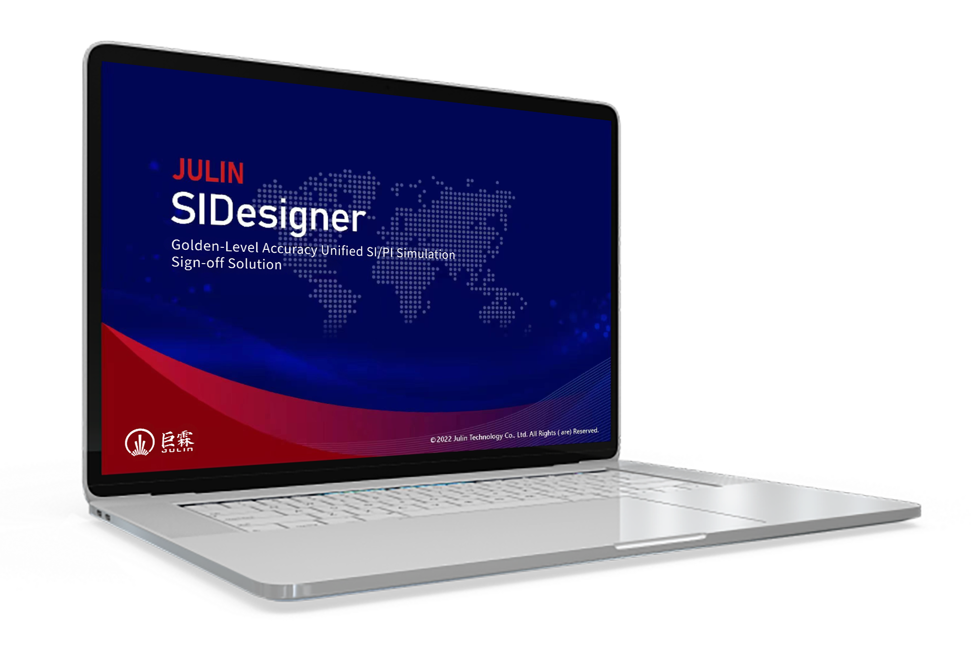
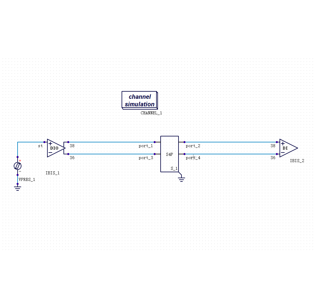
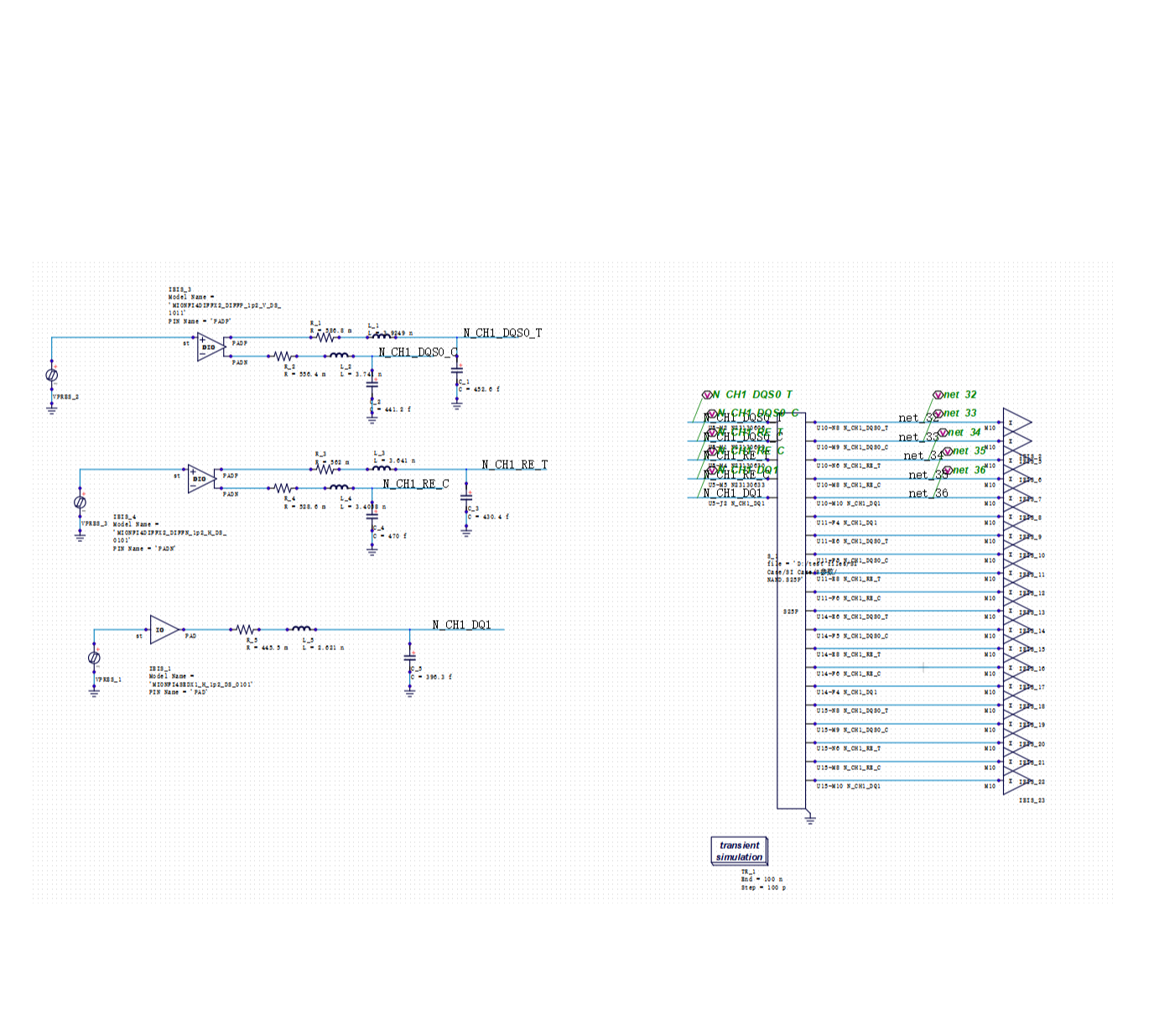
Julin Technology's current flagship product, SIDesigner, is a circuit-level simulation tool designed for this field.
In Deng Junyong's view, the industry often discusses whether domestic EDA tools can achieve “Golden” accuracy. However, the issue is not that simple.
“Golden” status is not established simply because an EDA vendor declares it.
A truly Golden tool must go through extensive customer validation.
Fundamental algorithms are, of course, important. For circuit simulation, many classical algorithms have existed for years, and the industry already has relatively mature theoretical foundations.
But writing the algorithms is only the starting point of EDA commercialization.
Deng pointed out that the real difficulty lies in the engineering work that follows.
Different customers, process technologies, interfaces, and design methodologies generate a large number of real-world cases. EDA tools must continuously identify problems, refine algorithms, and optimize models through these cases before eventually becoming stable commercial tools.
Therefore, Deng believes that for an EDA tool to become an industry-recognized “Golden” tool, it requires more than leading algorithms. It requires credibility built through years of accumulated customer cases.
This is also one of the most difficult challenges for domestic EDA.
The advantages of overseas EDA giants do not lie solely in their products. Over decades, large numbers of customers have built their own design flows, verification flows, and toolchains.
Once a tool enters an enterprise workflow, it is no longer just software. It becomes part of the entire R&D system.
In other words, what customers are actually purchasing is not simply a piece of EDA software, but a level of certainty that has been validated through a large number of projects.
This also explains why domestic EDA replacement is not easy.
2. Customer Stickiness Is Strong, but Domestic EDA Is Beginning to Gain Opportunities as the “Second Tool”
For Chinese EDA companies, one of the biggest practical challenges is that customers have already become accustomed to overseas tools.
Deng Junyong does not avoid this reality.
In his view, from the perspective of a chip design engineer, choosing to completely replace a mature tool that has been used for many years with a domestic alternative is not an easy decision in the short term.
“This kind of stickiness cannot be broken overnight.”
However, this does not mean that domestic EDA has no opportunities.
A very practical entry point is beginning to emerge: moving from “replacing the customer's first tool” to “becoming the customer's second tool.”
For chip companies, cross-validation using multiple tools is itself a relatively common method of risk control.
A customer may previously have purchased ten sets of overseas EDA tools, but may now be willing to allocate one or two positions for domestic EDA vendors to conduct validation, provide supplementary capabilities, or perform cross-validation.
For domestic EDA companies, this change is extremely important.
In the past, domestic tools might not even have had the opportunity to enter a customer's validation system.
Today, however, as long as a domestic EDA vendor can demonstrate its accuracy, performance, and service capabilities in a specific niche, it may gain a real entry point.
This is exactly the path Julin Technology is attempting to follow and gradually expand.
Deng also emphasized an easily overlooked issue: service response speed is itself part of an EDA product's competitiveness.
As chip design enters an era of rapid iteration, EDA simulation is no longer simply a “checking tool” used after a design is completed. It is increasingly becoming part of the design process itself.
Suppose a customer's product is scheduled for release tomorrow, but a simulation problem is discovered today.
If the EDA vendor requires a week to identify the problem, the customer's loss may not simply be one engineer's time. It may affect the entire product launch cycle.
Conversely, if a domestic EDA vendor can provide effective analysis more quickly, this service capability may become one of the reasons customers choose a domestic tool.
This is also the differentiation Julin Technology is attempting to establish:
Not only building the tool, but helping customers solve their problems.
3. From 112G SerDes to HBM and UCIe, SIDesigner Is Entering the High-Bandwidth Era
Based on currently disclosed application cases, Julin Technology's SIDesigner covers a relatively broad range of high-speed interfaces.
These include DDR, LPDDR5, SerDes, as well as HBM and UCIe in the advanced packaging field.
Behind this is a structural transformation taking place across the semiconductor industry:
Bandwidth is increasing, packaging is becoming more complex, and data transmission both within and between chips is becoming a major bottleneck for overall system performance.
In the past, chip design focused more heavily on transistor counts, logic functions, and operating frequency.
Today, with the development of AI chips and high-performance computing, technologies such as HBM, high-speed SerDes, Chiplets, and UCIe are becoming increasingly important parts of system design.
This means the importance of SI/PI simulation continues to grow.
For example, 112G SerDes has already entered practical design applications, while even higher speeds such as 224G are becoming the next direction of technological development.
As data rates increase, signal integrity challenges become increasingly prominent.
At this stage, relying solely on traditional engineering experience is becoming more difficult.
“In the past, when conducting simulations, engineers could often determine whether something had a problem based largely on personal experience,” Deng said.
However, the situation has changed in the era of advanced packaging and high-performance computing chips.
The design and tape-out costs of high-performance chips are continuing to increase, and engineers can no longer rely solely on experience to bear the final engineering risks.
As a result, the importance of simulation, verification, and Signoff has been further amplified.
Simulation tools are evolving from “design assistance tools” into risk-control tools within the chip design workflow.
This may be one of the reasons why the SI/PI simulation market is expected to continue growing over the coming years.
4. AI Is Entering EDA, but Julin Does Not Believe Every Simulation Requires a Large Model
AI is entering EDA, and this is a major industry trend.
However, in Deng Junyong's view, AI + EDA should not simply be understood as “putting a large model into an EDA tool.”
For simulation tools in particular, many problems do not inherently require generative AI.
Julin's current AI efforts are primarily focused on algorithm optimization, acceleration, adaptive workflow optimization, and improving the usability of engineering tools.
The reason is straightforward:
Many problems addressed by simulation tools involve improving search efficiency and workflow efficiency on top of physical solvers, rather than asking a large model to “generate” an answer.
Therefore, in Julin's approach, AI is more like an optimizer.
For example, AI can be used to search parameters based on existing data, optimize models, and explore design spaces, reducing large amounts of repetitive computation through machine learning.
This approach integrates more naturally with traditional simulation tools.
For AI applications involving customers' core design data, however, data security becomes another issue that must be addressed.
Chip companies' internal design data is often extremely sensitive.
A company's chip design data cannot simply be used for training and then potentially made available to competitors.
Therefore, Deng believes that the AI path for EDA in the future is unlikely to simply replicate the approach used by internet-scale large models.
A more practical approach may be:
General-purpose foundation models + fine-tuning on local private data + RAG + local or private deployment.
This approach makes it possible to leverage AI capabilities while reducing the risk of exposing core design data.
This is also a unique constraint that AI must address when entering EDA:
The AI transformation of EDA is first an engineering problem, and only then a model problem.
5. Advanced Packaging Is Hot, but the Underlying Logic of EDA Has Not Been Completely Rewritten
Over the past two years, advanced packaging, Chiplets, and 3D IC have become some of the hottest topics in the semiconductor industry.
As a result, many people have formed a view:
If packaging is becoming increasingly complex, does that mean EDA itself needs to be completely reconstructed?
Deng Junyong offered a relatively cautious answer.
Advanced packaging has indeed introduced new design and simulation requirements, but the underlying logic has not undergone a disruptive transformation.
For example, the scale of structures such as interposers and advanced packaging has changed, and design complexity has increased significantly. However, traditional back-end design tools, after appropriate adaptation, can still handle a considerable portion of the work.
The same is true for simulation.
With targeted adaptations, traditional simulation tools can also support many advanced packaging scenarios.
What has truly changed is primarily:
Scale, structure, interfaces, and workflow complexity.
It is not that the fundamental principles of EDA design and simulation have been completely rewritten.
This is also why the industry's current discussion of “multi-scale simulation” does not mean that a single simulation engine can seamlessly calculate everything from the nanometer scale to the millimeter scale.
Different scales often correspond to different computational models and different solver engines.
For example, package PCBs may involve dimensions on the scale of tens of micrometers, while interposers may operate at smaller scales. Power modeling inside a chip represents another category of problem altogether.
If every problem were solved using exactly the same electromagnetic algorithm, the computational scale would quickly become unacceptable.
Therefore, the real technical challenge is not simply pursuing “one tool that solves everything.”
Instead, the challenge is:
How to select the appropriate algorithms for different scales and different physical problems, and then connect the resulting data and models together.
This may be the real problem that advanced packaging EDA needs to solve.
6. The Next Stage of Domestic EDA Is Not About Being “Big and Comprehensive,” but About Building an Irreplaceable Local Advantage First
When discussing the future industrial landscape of domestic EDA, Deng Junyong did not avoid another reality:
Everyone wants to build full-flow EDA, but wanting to do so does not necessarily mean being able to achieve it.
He pointed out that EDA is a typical long-term accumulation industry.
If a company hopes to gradually expand from a niche tool into a complete design flow, it must first have a product capable of continuously generating revenue and supporting ongoing R&D investment.
Otherwise, as the product portfolio continues to expand, R&D pressure may instead become a burden for the company.
Therefore, Deng believes that a more practical path for domestic EDA companies may be:
First become sufficiently strong in one specialized area, and then gradually extend upstream and downstream.
Julin's choice of SI/PI simulation reflects this strategy.
Rather than attempting to replicate the complete product portfolio of overseas EDA giants from the beginning, the company has continued to accumulate capabilities around high-speed simulation, power integrity, signal integrity, and advanced packaging scenarios.
This path is not fast.
But the EDA industry was never an industry suited to pursuing short-term speed.
Especially in markets where “Golden” tools already exist, what domestic EDA truly needs to establish is a new system of trust.
From the first tool to the second tool.
From auxiliary verification to formal Signoff.
From one product to multiple workflows.
Every additional customer case effectively increases the credibility of domestic EDA.
Therefore, to understand where Julin Technology stands today, it may be more accurate to view the company not simply as a “domestic EDA replacement company,” but as:
A company attempting to gradually establish engineering credibility for domestic EDA tools through the specialized battlefield of high-speed simulation.
Domestic EDA Has Entered the Real “Deep Water”
In the past, the question facing domestic EDA was:
“Do we have it?”
Today, the question is increasingly becoming:
“Do customers dare to use it?”
And there is a long gap between those two questions.
Algorithms are only the first hurdle.
What follows includes real-world customer cases, customer validation, tool stability, Signoff capabilities, service response, ecosystem collaboration, and perhaps most importantly:
Customer trust.
This is why domestic EDA replacement is destined not to be a short-term product competition.
Particularly in rapidly evolving areas such as SI/PI, high-speed SerDes, HBM, UCIe, advanced packaging, and automotive-grade chips, EDA is moving beyond the role of “design assistance software” and increasingly becoming infrastructure within the chip R&D system.
The path Julin Technology has chosen is, in fact, very clear:
The company is not rushing to prove whether it can build a “big and comprehensive” EDA platform.
Instead, it is first going deep into the specialized field of high-speed simulation, strengthening its accuracy, customer cases, and customer service capabilities.
Because for domestic EDA, real replacement never begins on the day a product is launched.
It begins on the day a customer is willing to entrust its chip design to you for verification.


Recommended
-
 China's Domestic EDA Enters the “Deep Water”: How Is Julin Technology Opening a Path Through SI/PI Simulation?
 2026.09.08
 -
 AI-Era Simulation EDA: Where Is It Heading?
2026.09.02
AI-Era Simulation EDA: Where Is It Heading?
2026.09.02 -
 Julin-tech Wins "China IC Design Achievement Award: EDA Company with Annual Technical Breakthrough" for the Third Consecutive Year
2026.04.02
Julin-tech Wins "China IC Design Achievement Award: EDA Company with Annual Technical Breakthrough" for the Third Consecutive Year
2026.04.02 -
 Julin-Tech Hosts Inaugural SI/PI High-Level Tech Seminar
2026.01.26
Julin-Tech Hosts Inaugural SI/PI High-Level Tech Seminar
2026.01.26