











AI-Era Simulation EDA: Where Is It Heading?
-
 2026.09.02
Whether it is Kimi and OpenAI using LLMs to design chips, or the three major EDA giants using Agents to accelerate chip design, one fact has become undeniable: artificial intelligence has entered the EDA industry.
Junyong Deng, Deputy General Manager of Julin Technology (Shanghai) Co., Ltd., also pointed this out in his keynote speech at the recently held ICDIA 2026 Integrated Circuit Design Innovation Conference. While AI has already found many applications in the EDA field, the challenges that have emerged alongside these applications have also raised a number of questions.
Against this background, he used the impact of AI on simulation tools as an example to share his latest views on EDA in the era of artificial intelligence.

What Does AI Mean for EDA?
Junyong Deng pointed out directly that AI is not entering EDA only now. Long before the emergence of large language models, the EDA industry had already widely adopted intelligent technologies such as Design of Experiments (DOE), optimization algorithms, and heuristic search.
What is different today is that what is now referred to as AI EDA represents a new stage of development centered around Agents.
“The value of an Agent lies not only in making EDA tools more intelligent, but also in reshaping the entire chip design process to achieve improvements in both human productivity and overall efficiency,” said Junyong Deng.
He pointed out that intelligent algorithms in traditional EDA primarily serve individual tools, such as placement and routing optimization, parameter search, and timing optimization. Essentially, they improve the performance of a specific tool at a particular point in the workflow.
Today's EDA Agents, however, are attempting to take on higher-level responsibilities: understanding engineers' intentions, automatically calling multiple EDA tools, orchestrating design workflows, and even completing verification and iteration.
In Junyong Deng's view, AI-enabled EDA can be divided into two levels.
The first is the tool level, where Agents improve the performance and operational efficiency of individual tools.
The second is the workflow level, where Agents connect front-end, back-end, verification, and other stages to achieve automated workflow orchestration and collaborative optimization.
For chip design companies, the most direct value is improved human productivity. In other words, the core criterion for measuring an EDA Agent is not the size of the model, but the speed of the closed loop—whether verification and decision-making can be completed with fewer people and in less time.
For this reason, Junyong Deng believes that the true value of an AI Agent in EDA is to reconstruct the design workflow and improve exploration efficiency on the premise of traceability.
Specifically, this can be summarized in three points:
1. EDA Agents need three layers of capabilities:
The interaction and orchestration layer is responsible for understanding requirements and organizing workflows; the knowledge and data layer provides design experience and rules; while the engine and model layer contains the physical solving core of traditional EDA, which is also the part that is currently most difficult for AI to replace.
2. Traceability is more important than automation:
A mature EDA Agent must not only be able to complete tasks automatically, but also record every decision, support verification, and provide traceability. Otherwise, once a design error occurs, it will be difficult to locate the problem.
3. AI will improve efficiency in the short term, while it may change the way designs are created in the long term:
In areas such as coding, where rules are clearly defined, AI already has relatively strong replacement capabilities.
During the presentation, Junyong Deng pointed out that in scenarios such as chip design, system verification, and SI/PI simulation, AI currently mainly performs automated orchestration, expands the simulation exploration space, and accelerates optimization, rather than replacing the underlying solvers.
A truly meaningful form of “AI-designed chips” will still require further technological maturity.
For this reason, Junyong Deng believes that simulation EDA has reached a stage where proactive transformation is necessary.
What Will Change—and What Will Not—for Simulation EDA?
When talking about EDA, we may be particularly familiar with EDA tools responsible for “drawing” the chip. However, as core tools responsible for verification within the chip design process, simulation EDA is equally important.
Through circuit models and physical solvers, simulation EDA simulates real operating conditions such as signal integrity (SI), power integrity (PI), and electromagnetic (EM) effects before chip fabrication, helping identify potential problems involving high-speed interfaces, power noise, crosstalk, bit error rate, and other factors in advance.
In other words, the responsibility of simulation EDA is to prove before manufacturing that a design can “really operate reliably.”
It is also an indispensable part of advanced chip development involving advanced packaging, HBM, UCIe, SerDes, and other high-speed technologies.
As the cost of chip fabrication continues to increase, the importance of simulation EDA is also growing.
Facing the impact of the AI wave, Junyong Deng emphasized in his presentation:
“AI will not replace physics solvers, but will change how solvers are invoked and verified.”
As he explained, AI is well suited to rapidly searching parameter combinations, screening candidate solutions, identifying anomalies, and organizing results in complex design spaces.
It can help engineers explore more possibilities and reduce a large number of low-value repetitive attempts.
However, final signoff results still require deterministic calculations from SPICE, electromagnetic, thermal, and other physics solvers.
Especially when dealing with new structures, new materials, and extreme operating conditions that are not covered by training data, engineering teams must know what inputs produced each result, which tool version and solver settings were used, and whether the same conclusion can be reproduced by running the process again.
For simulation EDA in the AI era, Junyong Deng believes that four practical issues cannot be ignored:
Customer design data cannot be freely aggregated, and failure samples are particularly scarce;
Model hallucinations and inputs outside the training scope may lead to incorrect judgments;
Interfaces and data semantics across legacy tools are not unified;
Once AI enters production workflows, IP isolation, permissions, and responsibility for results must have clear mechanisms.
Therefore, in Junyong Deng's view, a more appropriate relationship between AI and simulation EDA is an “exploration–verification–iteration” loop:
AI proposes candidate solutions and anomaly hypotheses, while physics solvers perform verification. The verification results are then returned to AI for the next round of task adjustment.
AI improves exploration efficiency, while physics solvers provide the basis for final engineering decisions.
This view also guides the evolution of Julin Technology's product development roadmap.
Julin Technology's Path Forward
As a company focused on EDA simulation and signoff for chips, advanced packaging, and systems, Julin Technology has established a product portfolio covering three major simulation domains: circuit, electromagnetic, and system simulation.
The portfolio includes the True-SPICE simulation platform PanosSPICE, one-stop SI/PI simulation platform SIDesigner, full-board PCB simulation platform ASCENEXT, 3D electromagnetic simulation tool EMArtist, and power electronics simulation platform PowerExpert.
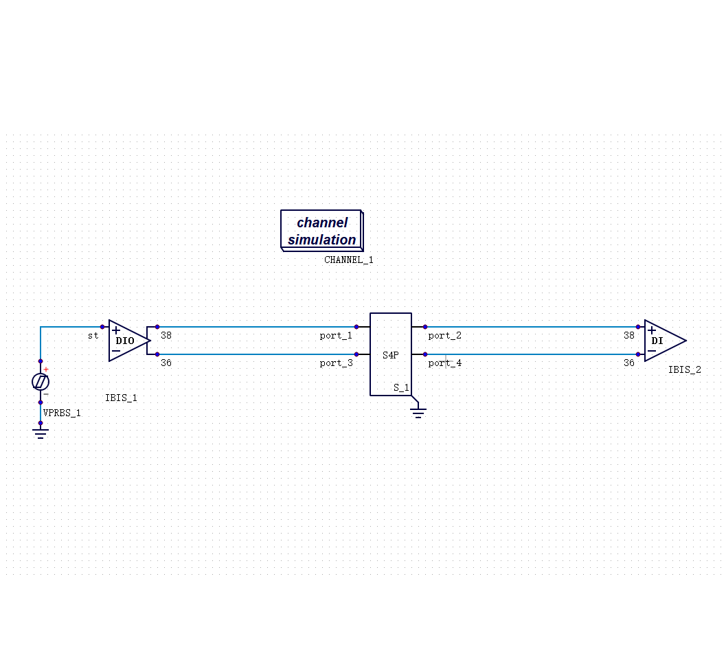
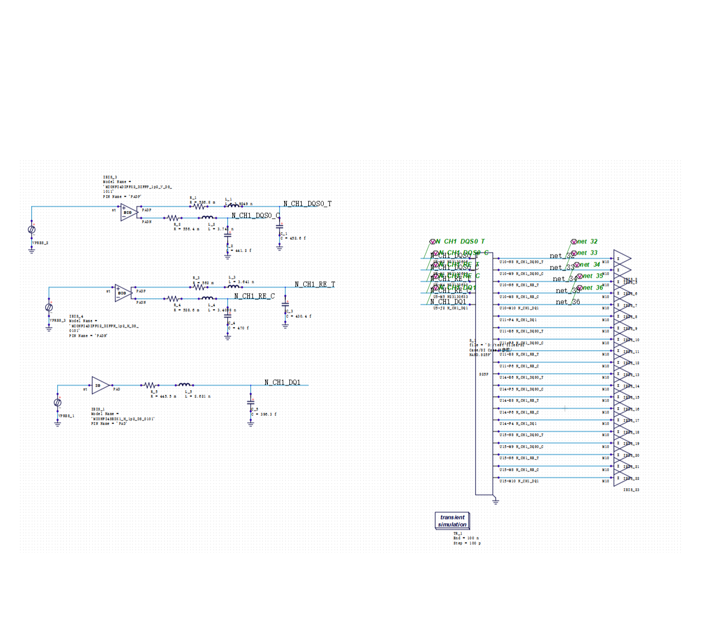
Among these products, the company's flagship product, SIDesigner, focuses on high-speed signal and power integrity (SI/PI) simulation and covers mainstream high-speed interfaces such as HBM, UCIe, DDR5/LPDDR5X, and SerDes.
During ICDIA, Julin Technology also officially launched a new technology introduced in the SIDesigner 3.0 stage: SIDesigner Transient-BER.
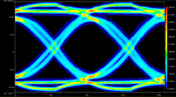
It is designed for low-bit-error-rate verification under nonlinearity, crosstalk, TX Jitter, and other conditions in high-speed interfaces, providing engineers with a new approach that balances solution accuracy and computational efficiency.
By combining critical transient simulation with statistical computation, Transient-BER extracts nonlinear response boundaries through a limited number of transient calculations, constructs a system-level nonlinear PDF, and ultimately calculates BER through integration.
This avoids long-duration exhaustive pattern simulation while significantly reducing the computational workload of ultra-low-BER simulation while maintaining accuracy.
Junyong Deng also revealed that another electromagnetic simulation product from the company, EMArtist, is currently under development and is planned for gradual release in the fourth quarter of this year. Together with SIDesigner, it will build a simulation chain from electromagnetic modeling to system signoff.
Regarding the company's investment in AI EDA, Junyong Deng clearly stated that Julin's strategy is not to have large language models replace simulation.
At present, Julin's AI efforts mainly focus on algorithm optimization, acceleration, adaptive workflow optimization, and improved tool usability.
At this stage, customer data has not been used for model training, while the underlying physical solving continues to rely on high-precision simulation engines.
Looking ahead, according to Julin Technology, in 2026, the company will focus on building callable product capabilities and a data evaluation foundation, unifying core function interfaces, task deion methods, and result-recording methods, so that existing tools have the engineering foundation required for reliable AI invocation.
In 2027, Julin plans to launch Copilot and Check Agent capabilities for configuration generation, report summarization, and rule checking, initially validating single-scenario closed loops in tasks with clearly defined boundaries.
In 2028, the company will further advance the SI Signoff Agent toward cross-tool collaboration and the generation of candidate Engineering Change Order (ECO) solutions, while improving rollback, reproducibility, and human review mechanisms.
The SI Signoff Agent is the first minimum viable closed loop planned by Julin Technology.
It will focus on the signal integrity signoff process and connect design import, link identification, task configuration, solver execution, rule checking, problem localization, ECO candidate generation, and report generation.
The goal is to ensure that every calculation has a clear basis and every conclusion can be reproduced within clearly defined human-review boundaries, rather than simply adding a chat window to an EDA tool.
Conclusion
Regarding the future of simulation EDA, Junyong Deng stated that the competitive advantage in the AI era does not lie in being the first to build a “large and comprehensive” closed-loop system, but in making individual tools as capable as possible.
On the one hand, companies should make full use of Agents to improve simulation workflows, design optimization, and engineering efficiency while continuously strengthening underlying solver capabilities.
On the other hand, individual tools must have open interfaces and strong collaboration capabilities so that they can be flexibly called by other tools and Agents and become key nodes within the ecosystem.
In addition, result trustworthiness and process traceability are fundamental requirements for AI EDA. Every decision must be verifiable and traceable.
“For simulation EDA, the changes brought by AI will ultimately be reflected in engineering results: Can the workflow deliver verifiable conclusions faster and more reliably? Future competition will also revolve around this ability to continuously deliver such results,” Junyong Deng concluded.
(Source: Compiled from BusinessKorea)


Recommended
-
 China's Domestic EDA Enters the “Deep Water”: How Is Julin Technology Opening a Path Through SI/PI Simulation?
 2026.09.08
 -
 AI-Era Simulation EDA: Where Is It Heading?
2026.09.02
AI-Era Simulation EDA: Where Is It Heading?
2026.09.02 -
 Julin-tech Wins "China IC Design Achievement Award: EDA Company with Annual Technical Breakthrough" for the Third Consecutive Year
2026.04.02
Julin-tech Wins "China IC Design Achievement Award: EDA Company with Annual Technical Breakthrough" for the Third Consecutive Year
2026.04.02 -
 Julin-Tech Hosts Inaugural SI/PI High-Level Tech Seminar
2026.01.26
Julin-Tech Hosts Inaugural SI/PI High-Level Tech Seminar
2026.01.26