


ICChina | Overcoming Chiplet Simulation Bottlenecks – Julin Technology’s SIDesigner Platform Builds a High-Precision Simulation "Core" Foundation
-
 2025.12.02
From November 23 to 25, the China International Semiconductor Expo (IC China) was held at the China National Convention Center in Beijing. As the most authoritative annual event in China's semiconductor industry, IC China has successfully hosted twenty-one editions since its inception in 2003 and has become a top-tier industry brand event and a benchmark in the field.
Junyong Deng, Vice President of Julin Technology, was invited to attend the conference and delivered a keynote speech titled "SI/PI Simulation Challenges in Chiplet Interconnects and Domestic Sign-off Solutions" at a technical forum.
Addressing the co-simulation challenges of Chiplet design in signal and power integrity, Junyong Deng systematically presented Julin Technology's technical solution based on the SIDesigner platform. By establishing a complete simulation chain from electromagnetic modeling to system sign-off, the solution has achieved comprehensive benchmarking against international industry leaders, providing a highly reliable sign-off verification tool for complex heterogeneous integration.
Chiplet Reshapes the Semiconductor Ecosystem
Faced with the physical and economic bottlenecks of process scaling and global supply chain uncertainties in the post-Moore era, the semiconductor industry is shifting from transistor density to system-level integration, sparking a design paradigm revolution centered on Chiplet.
By deconstructing the traditional "single-chip" model, Chiplet breaks down complex SoCs into modular "chiplets" that can be independently manufactured and functionally optimized, enabling heterogeneous integration and system-level PPA optimization. Its driving forces lie in: first, heterogeneous process integration, allowing units such as CPUs, GPUs, and memory to adopt their optimal processes; second, balancing cost and yield by using advanced processes for core units and mature processes for others; third, modular chiplets can be reused across products, promoting agile design evolution, rapid iteration, and deep customization.
Advanced Packaging Builds the Chiplet "Highway"
The Chiplet vision relies heavily on advanced packaging technologies. While basic multi-chip modules (MCMs) can achieve fundamental multi-chiplet integration, realizing its full potential—especially meeting the high-bandwidth, low-latency Die-to-Die interconnect requirements—requires 2.5D/3D advanced packaging technologies such as CoWoS and EMIB.
These technologies provide interconnect capabilities far exceeding traditional substrate routing density through silicon interposers, silicon bridges, or microbumps, serving as the "highway" connecting functional chiplets. It is this bridge built by advanced packaging that enables tight collaboration between computing chiplets and high-bandwidth memory (HBM), transforming the "system LEGO" from a conceptual blueprint into high-performance reality.
Simulation Complexity in Multi-Physics Coupling
Multi-physics coupling dramatically increases packaging design complexity. The design focus has expanded from single chips to full-package systems, with mechanical stress, thermal management, signal integrity, and power integrity issues intertwining, presenting unprecedented simulation challenges.
Among these, signal integrity directly impacts system stability. Its core difficulty lies in cross-scale electromagnetic modeling—from sub-micron interposer routing to tens-of-micron substrate traces. The scale variation imposes extreme requirements on simulation tool meshing and algorithms. As Die-to-Die interface rates continue to rise, crosstalk and loss under high routing density, combined with simplified IO designs for low power, significantly compress timing margins. Simulation tools must not only possess SPICE-level accuracy but also support SI/PI co-analysis to accurately assess the impact of power noise on timing.
Power integrity also faces challenges: AI computing units generate burst currents, periodically impacting the power network. Meanwhile, core and IO power for high-speed interfaces must carry high currents while maintaining low noise. Electromagnetic modeling of the power network faces similar cross-scale challenges and requires time-domain simulation of worst-case current scenarios. Successful PI simulation relies on precise frequency-domain optimization of power distribution network impedance and thorough validation of voltage fluctuations caused by transient load changes through transient simulation.
Closed-Loop Verification with High-Precision EDA Toolchain
To address the multi-physics simulation challenges brought by Chiplet technology, the EDA industry is building comprehensive solutions from physical structures to system performance.
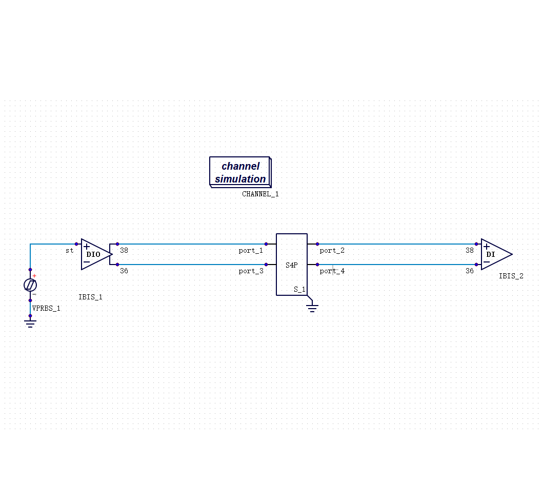
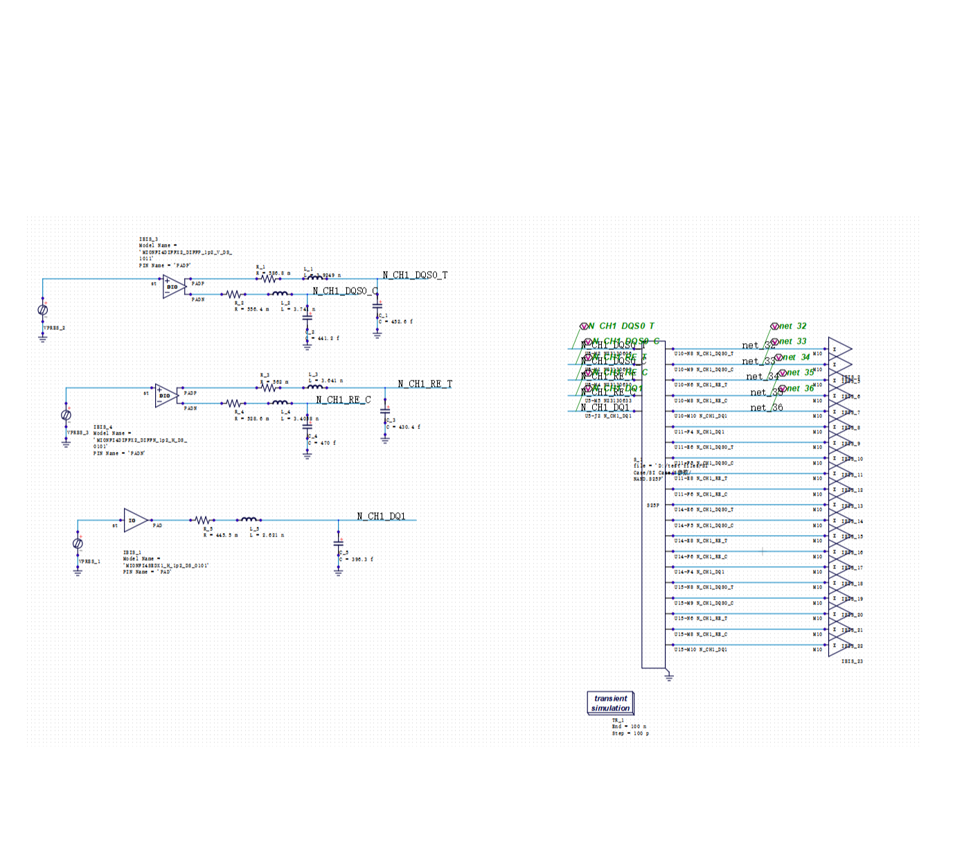
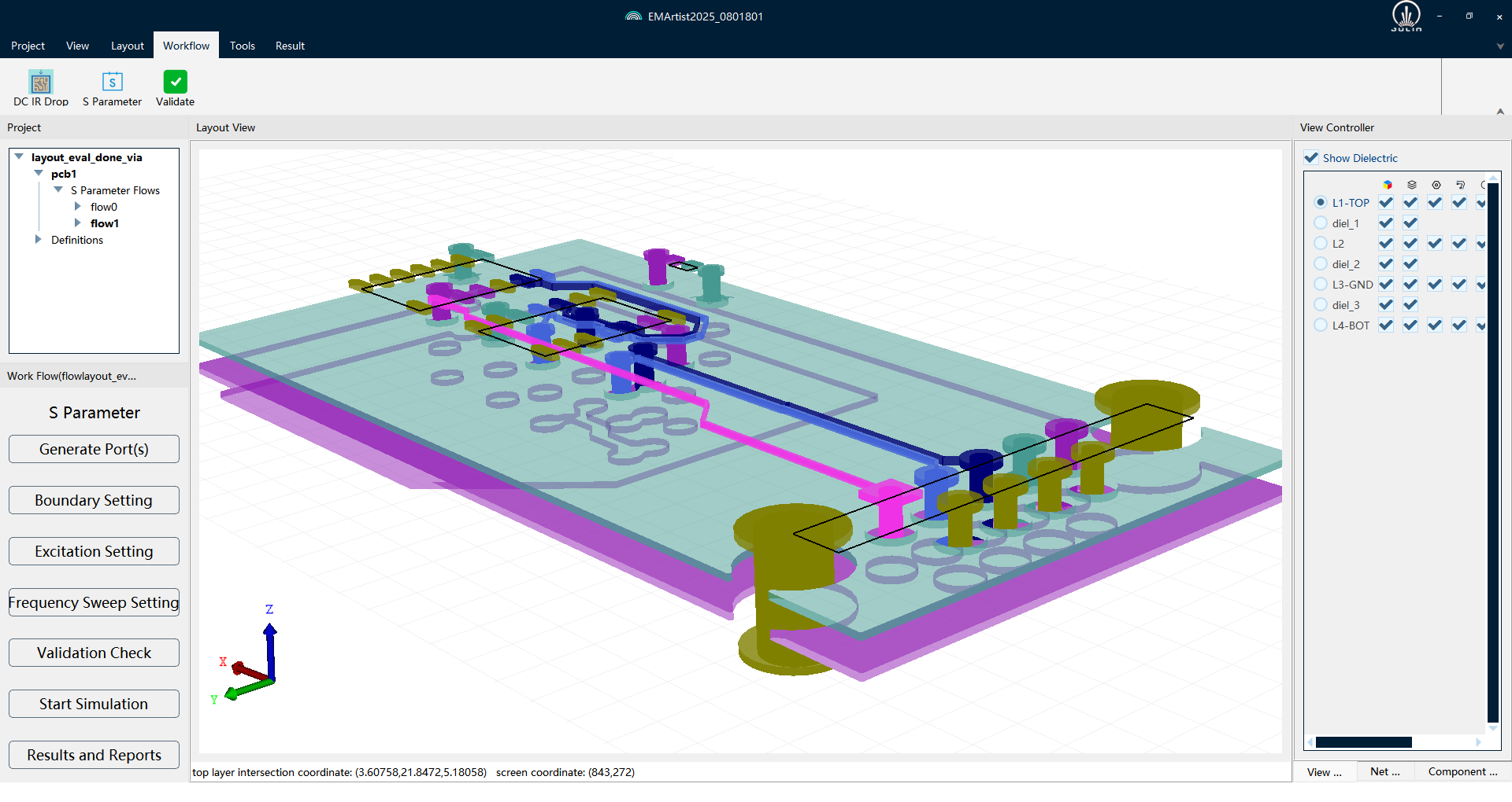
Taking Julin Technology's SIDesigner platform as an example, a complete simulation chain is established in collaboration with EMArtist: EMArtist focuses on high-precision electromagnetic modeling of 3D packaging structures (Interposer, Bump, TSV, PKG, PCB, etc.), extracting high-precision broadband S-parameter models and SPICE models; SIDesigner handles final system-level sign-off by integrating TX/RX chip models with passive links to perform SI/PI co-simulation, comprehensively evaluating channels, eye diagrams, and power noise (IR Drop, SSN), thus achieving a precise verification loop from physical prototype to system performance sign-off.
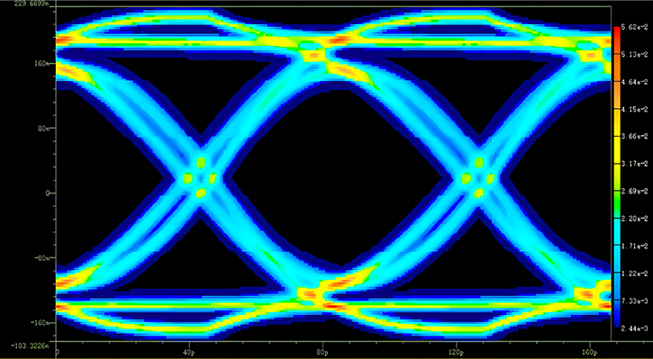
In practical scenario validation, SIDesigner's key eye diagram parameters (eye height, eye width) in high-speed interface scenarios such as DDR4 transient simulation and PCIe6 channel simulation show differences of less than 2% compared to international benchmark tools. Its performance has reached the industry's Golden-level accuracy standard. The platform comprehensively covers simulation requirements for parallel interfaces such as DDR/HBM and SerDes interfaces such as PCIe/MIPI, providing two sets of solutions: True-SPICE time-domain simulation and Channel Simulation. Its TJSPICE simulator fully benchmarks against industry Golden-level simulators in convergence and stability, with superior accuracy in some scenarios.
Junyong Deng stated that, based on a clear product roadmap, SIDesigner plans to achieve comprehensive application benchmarking with industry Golden-level solutions by 2025 and build an industry-leading SI/PI simulation platform within three years. This development path marks its progression from "usable" to "user-friendly," providing critical simulation verification capabilities for the large-scale application of Chiplet technology and serving as an important practice for breakthroughs in semiconductor industry simulation technologies under complex heterogeneous integration scenarios.
Looking ahead, Julin Technology will always uphold its mission of "Precise Simulation, Empowering the Future," continuously deepening its expertise in "circuit" and "electromagnetic" simulation technologies. Closely围绕 industry frontier demands, we will continue in-depth collaboration with strategic customers and industry chain partners, constantly creating and launching new industry benchmark products. Through continuous technological iteration and ecosystem development, Julin Technology will connect the dots, expand from lines to surfaces, and build industry-leading EDA solutions, contributing to the advancement and leadership of China's domestic EDA industry.


Recommended
-
 AEIF 2026: Julin Tech’s Beijie Qian on Why "Simulation Pass" Does Not Equal "Mass Production Yield"
 2026.05.22
 -
 IIC Shanghai | High-Speed Interface SI Signoff: Precision Limitations of Statistical Domain Algorithms and Path Reconstruction
2026.04.02
IIC Shanghai | High-Speed Interface SI Signoff: Precision Limitations of Statistical Domain Algorithms and Path Reconstruction
2026.04.02 -
 Julin Technology Showcases Unified CPS SI/PI Simulation Platform at ICCAD
2025.12.02
Julin Technology Showcases Unified CPS SI/PI Simulation Platform at ICCAD
2025.12.02 -
 Jiaxin Sun , Founder of Julin: Empowering High-Fidelity System Design with SIDesigner, a Golden-Level Precision SI/PI Sign-off Platform
2025.12.02
Jiaxin Sun , Founder of Julin: Empowering High-Fidelity System Design with SIDesigner, a Golden-Level Precision SI/PI Sign-off Platform
2025.12.02