












Advanced Packaging SI/PI Simulation: From 3D Electromagnetic Modeling to Chip–Package–PCB Co-Simulation
-
 2026.08.26
Abstract: Chiplets, HBM, and UCIe are extending high-speed links across dies, interposers, packages, and PCBs. Model and boundary-condition deviations introduced by segmented simulation can affect system-level decisions. This article introduces how EMArtist and SIDesigner connect 3D electromagnetic modeling with system-level SI/PI analysis to build an end-to-end verification workflow for advanced packaging.
On August 21, the “Advanced Packaging and EDA Collaborative Innovation” session of the China Integrated Circuit Innovation Application Conference & Exhibition (ICDIA 2026) was held in Nanjing. Beijie Qian, Product Director at Julin Technology, was invited to attend and deliver a keynote presentation titled “One-Stop SI/PI Simulation Platform for Advanced Packaging Design.”

Focusing on the design changes brought by 2.5D/3D packaging, Chiplets, HBM, and UCIe, Beijie Qian analyzed signal integrity (SI) and power integrity (PI) challenges in advanced packaging and introduced Julin Technology’s one-stop SI/PI simulation platform consisting of EMArtist and SIDesigner.
In his presentation, he pointed out that advanced packaging has connected chip dies, interposers, package substrates, and PCBs into a complete system. Any deviation in the model or boundary conditions at any stage may affect the final link evaluation. The traditional approach of performing simulations separately at the chip, package, and board levels is increasingly facing challenges in connecting these stages.
Advanced Packaging Brings SI/PI into the Early Stages of Architecture Design
From Fan-out and 2.5D silicon interposers to 3D vertical stacking, HBM, CoWoS, and UCIe Chiplet interconnects, packaging has expanded from basic interconnection to heterogeneous integration, high-bandwidth data transmission, and high-power delivery.
These capabilities are concentrated within smaller physical spaces, causing previously separate electrical issues to become increasingly interconnected. If high-speed link eye diagrams, bit error rate, power noise, or power delivery network design fails to meet target requirements, it may directly limit system bandwidth and the feasibility of the packaging solution.
Therefore, SI/PI needs to be introduced during the architecture design stage rather than being treated as a conventional verification task after layout completion.
For signal integrity, one of the primary challenges comes from cross-scale modeling. A single high-speed link may simultaneously include sub-micron RDL, silicon interposers, TSVs, micro-bumps, package substrates, and PCB traces.
The dimensions, materials, and electromagnetic characteristics of these structures vary significantly. If segmented modeling is overly simplified at the interfaces, parasitic parameters that affect system-level results may be lost.
As RDL routing density increases, electromagnetic coupling and crosstalk between traces can further reduce the effective eye opening. As the data rates of interfaces such as UCIe and XSR continue to increase, the unit interval becomes shorter, leaving increasingly limited margins for timing deviations and noise.
At the same time, I/O drivers are constrained by the system power budget and cannot simply compensate for channel loss by increasing signal swing.
Power integrity also needs to be analyzed across the complete system. AI and high-performance computing chips feature large Core power currents and rapid dynamic changes. Fixed-frequency computational workloads may also create specific noise patterns within the power delivery network.
Noise on the power supply of high-speed interface I/Os can further affect signal eye diagrams and jitter performance. In such scenarios, performing SI and PI analysis separately makes it difficult to capture the combined impact of simultaneous switching noise and worst-case data patterns.
EMArtist Handles Physical Modeling, While SIDesigner Performs System-Level Simulation
To address the cross-scale and multi-level interconnection challenges of advanced packaging, Beijie Qian introduced the collaborative solution combining Julin Technology’s EMArtist and SIDesigner.
EMArtist is a 3D full-wave electromagnetic field solver for PCB and IC packaging. It is responsible for electromagnetic modeling of structures such as silicon interposer traces, TSV arrays, micro-bumps, complex routing, and PDNs.
It extracts broadband S-parameter models and uses current-distribution and spatial electromagnetic-field analysis to identify potential risks.
Its role is to convert the physical structures of advanced packaging into high-accuracy models that can be used for system-level simulation.
SIDesigner takes over these interconnect and device models and performs system-level SI/PI simulation across the chip, package, and PCB.
The platform supports high-speed parallel and serial interfaces as well as power integrity analysis, and can be used to evaluate link performance under different structural parameters and operating scenarios.
The two tools address different tasks: EMArtist handles underlying physical structures and parasitic effects, while SIDesigner determines whether signal and power integrity metrics meet design requirements after these models are integrated into the complete system.
Through model handoff, Interposers, package substrates, and PCBs can be incorporated into the same simulation workflow.
From Physical Models to System Results: The Key Is Workflow Integration
Advanced packaging simulation typically involves both 3D electromagnetic modeling and system-level circuit analysis.
If these two types of tasks are completed through separate workflows, engineers need to repeatedly verify material properties, boundary conditions, port definitions, and version information during model handoff.
As packaging structures become more complex, any inconsistency can propagate into subsequent system simulations and affect the final evaluation.
The combination of EMArtist and SIDesigner provides a workflow covering physical structure modeling, interconnect model extraction, and system-level SI/PI analysis, enabling engineers to evaluate the complete link based on corresponding structures and models.
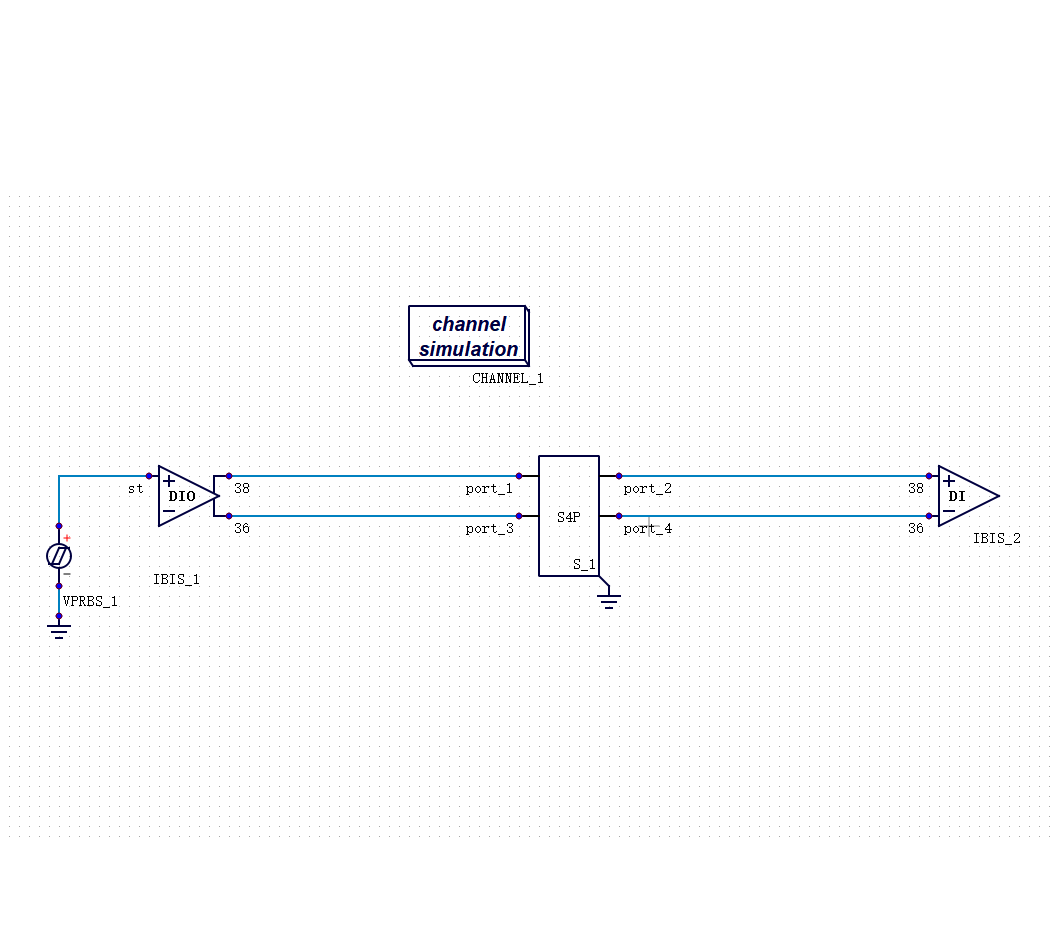
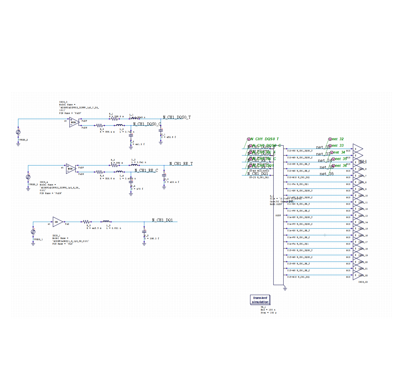
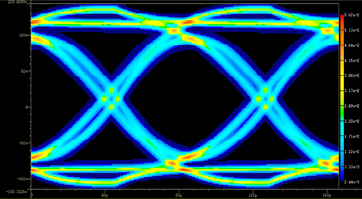
The presentation also demonstrated SI simulation cases involving three types of high-speed interfaces: LPDDR5, HBM3, and XSR.
These cases covered high-speed parallel memory, high-bandwidth memory within advanced packaging, and high-speed PAM4 interconnect scenarios, respectively, demonstrating how SIDesigner can be applied to different types of high-speed links.
Beijie Qian believes that collaboration between advanced packaging and EDA ultimately needs to be implemented through the integration of structures, models, solvers, and verification workflows.
Only by connecting these stages can design teams evaluate whether packaging structures and interconnect solutions meet performance requirements from the perspective of the complete system.
From Automated Simulation to Intelligent Optimization
Looking toward future product development, Julin Technology will continue to improve SI/PI simulation capabilities for scenarios including 2.5D/3D heterogeneous integration, UCIe interconnects, and HBM memory, while advancing AI-assisted automated DOE and intelligent parameter optimization Agents to explore structural and parameter combinations more efficiently.
Beijie Qian also pointed out that simulation and verification for advanced packaging require collaboration among wafer manufacturers, OSATs, chip design companies, EDA vendors, and research institutions.
Real-world structures, material parameters, design rules, simulation models, and test results need to be continuously aligned in order to gradually establish advanced packaging simulation methodologies and verification standards suitable for the local industry chain.
For chip designs moving toward 2.5D/3D packaging, Chiplets, and high-bandwidth interconnects, the scope of SI/PI simulation has expanded to the complete link spanning the chip, package, and system.
Julin Technology aims to provide one-stop tool support for this complete link through the collaboration of EMArtist and SIDesigner, covering the workflow from physical modeling to system-level analysis.


Recommended
-
 AEIF 2026: Julin Tech’s Beijie Qian on Why "Simulation Pass" Does Not Equal "Mass Production Yield"
 2026.05.22
 -
 IIC Shanghai | High-Speed Interface SI Signoff: Precision Limitations of Statistical Domain Algorithms and Path Reconstruction
2026.04.02
IIC Shanghai | High-Speed Interface SI Signoff: Precision Limitations of Statistical Domain Algorithms and Path Reconstruction
2026.04.02 -
 Julin Technology Showcases Unified CPS SI/PI Simulation Platform at ICCAD
2025.12.02
Julin Technology Showcases Unified CPS SI/PI Simulation Platform at ICCAD
2025.12.02 -
 Jiaxin Sun , Founder of Julin: Empowering High-Fidelity System Design with SIDesigner, a Golden-Level Precision SI/PI Sign-off Platform
2025.12.02
Jiaxin Sun , Founder of Julin: Empowering High-Fidelity System Design with SIDesigner, a Golden-Level Precision SI/PI Sign-off Platform
2025.12.02