


Beyond Moore’s Law: Navigating SI/PI and Multi-physics Challenges in Chiplet Heterogeneous Integration
-
 2025.10.29
As semiconductor processes approach their physical limits, relying solely on process node scaling is no longer sufficient to meet the surging demands for computing power and energy efficiency in fields like Artificial Intelligence (AI) and High-Performance Computing (HPC). Against this backdrop, Chiplet technology has emerged as a pivotal "More-than-Moore" heterogeneous integration solution. By integrating modular chips of varying processes and functions into advanced packaging, Chiplets have become the core pathway to addressing the challenges of high bandwidth, low latency, and low power consumption.
However, this architecture extends design complexity from a single silicon wafer to the entire packaging system. It interweaves multi-physics issues—including mechanical stress, thermal management, Signal Integrity (SI), and Power Integrity (PI)—creating unprecedented simulation and verification hurdles.
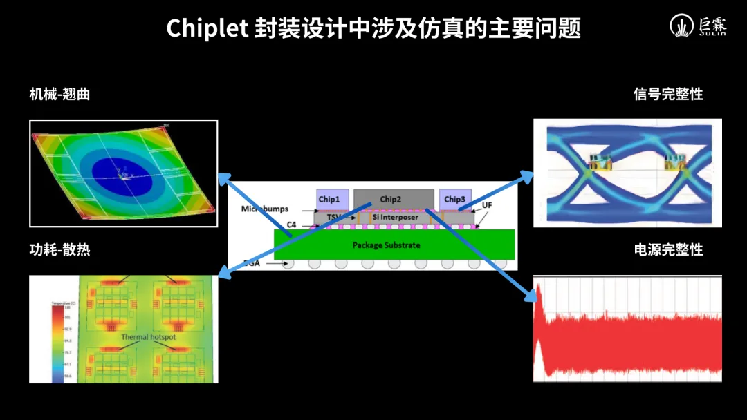
I. Multi-physics Coupling: Redefining Complexity in Chiplet Packaging
Advanced packaging structures, such as 2.5D and 3D ICs, significantly increase integration density but also introduce pronounced multi-physics coupling effects.
Mechanical warpage has intensified due to larger package sizes, a diverse range of materials, and concentrated thermal stress. Achieving high simulation accuracy for warpage depends heavily on precise modeling of production processes and material properties.
Thermal management challenges arise from the superposition of power consumption across multiple dies and localized high heat density. Simulation requires the construction of a complete thermal resistance network, spanning from internal chip modules to system-level cooling paths. These mechanical and thermal effects further alter the electrical characteristics of transmission lines, mandating that pure signal analysis give way to multi-physics co-simulation.
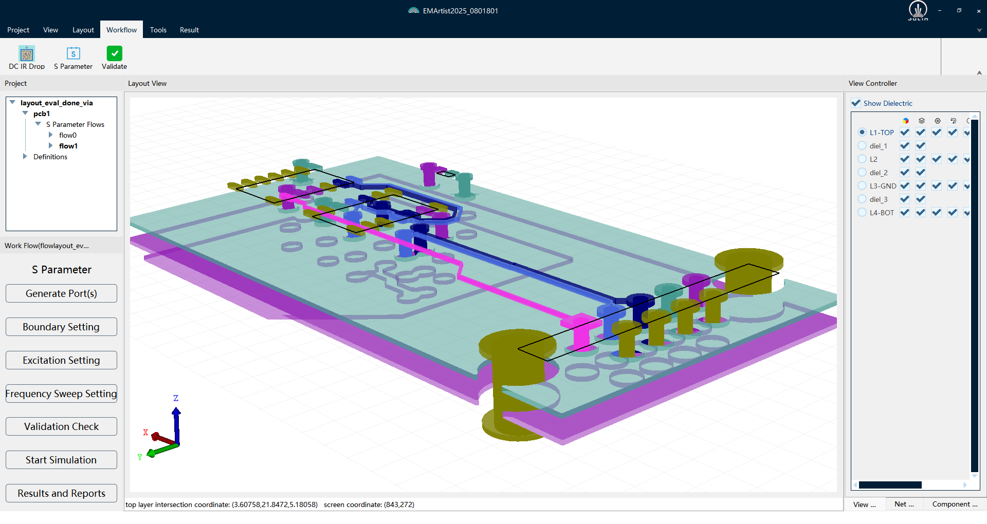
Among these challenges, Signal Integrity (SI) is particularly critical as it directly impacts system stability. The primary obstacle is the difficulty of cross-scale electromagnetic (EM) modeling. Within the same package, interconnect structures range from sub-micron silicon interposer routing to tens-of-microns organic substrate traces. This scale disparity pushes the meshing capabilities and algorithmic precision of EM simulation tools to their absolute limits.
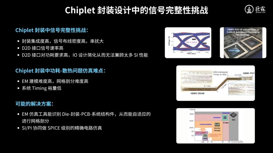
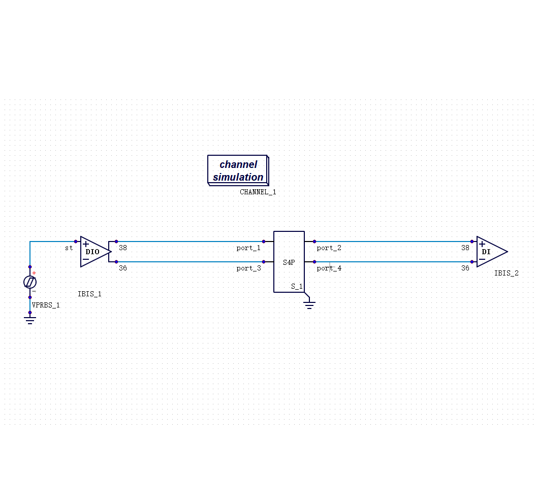
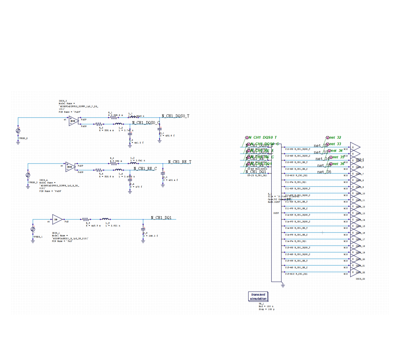
Simultaneously, Die-to-Die (D2D) interface data rates continue to climb. Under high routing density, severe crosstalk and transmission loss—combined with simplified I/O designs optimized for low power—drastically compress signal timing margins. This requires simulation tools to provide not only SPICE-level circuit accuracy but also SI/PI co-analysis capabilities to precisely evaluate the impact of power supply noise on sensitive timing.
Power Integrity (PI) faces equally stern tests. Computational units in AI applications generate burst currents at specific frequencies, creating periodic shocks to the Power Delivery Network (PDN). Core and I/O power supplies for high-speed interfaces must maintain ultra-low noise levels while carrying heavy currents.
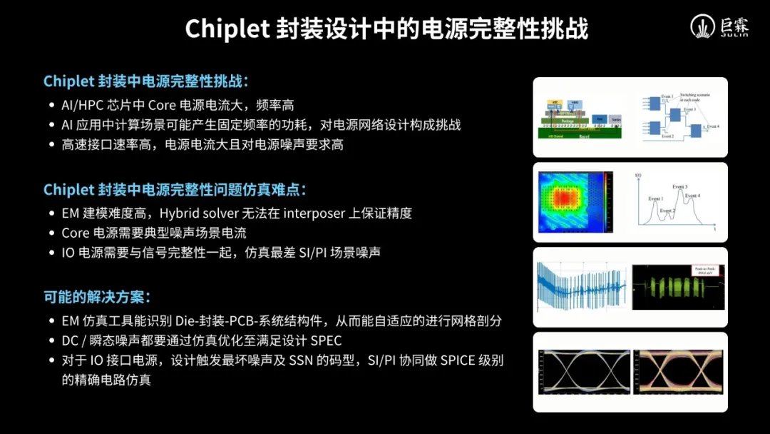
The difficulty lies in the fact that EM modeling of the power network faces the same cross-scale challenges as the signal network. Furthermore, it requires simulating the worst-case operating scenarios in the time domain. Successful PI simulation depends on the precise optimization of the PDN's frequency-domain impedance and thorough verification of voltage fluctuations triggered by load transients.
II. Precision vs. Efficiency: Driving the Evolution of EDA Toolchains
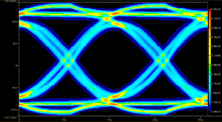
The industry currently faces a dilemma between long transient simulation and statistical simulation. Long transient simulation authentically reflects physical characteristics and serves as the baseline for accuracy, but its computational cost becomes unbearable as signal rates and channel lengths increase. While statistical eye diagram algorithms can compress simulation time from weeks to minutes, their inherent systematic errors can no longer be ignored in the context of Chiplet designs, where timing margins are extremely tight.
Addressing these challenges requires a comprehensive evolution of the simulation technology stack. Industry leaders are exploring pathways such as high-fidelity circuit models, high-precision EM field simulation, and hybrid solvers to tackle cross-scale modeling.
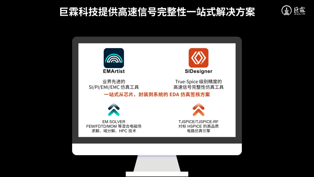
Julin-tech’s SIDesigner platform is a prime example of this evolution. By integrating circuit-level and statistical simulation solvers, SIDesigner aims to balance the demand for precision and efficiency in SI/PI co-simulation. It specifically addresses traditional pain points such as meshing adaptability and statistical eye diagram accuracy.
Conclusion: System-Level Simulation as the New Battlefield
Chiplet technology has shifted the battlefield of chip design from a single wafer to the entire packaging system. Signal and power integrity are no longer isolated design steps; they are system-level issues deeply coupled with mechanical and thermal factors.
Breaking through the barriers of cross-scale EM modeling and achieving high-efficiency, high-precision multi-physics co-simulation is key to the continued evolution of Chiplet technology and the release of its full performance potential. The industry’s expectations for next-generation EDA tools are focused on their ability to bridge the gap between chip, package, and system simulation under increasingly rigorous sign-off standards.
We invite you to click [Software Trial] to apply for a trial of our latest simulation tools. If you have any questions during the process, please contact our technical support team. We look forward to collaborating with you!


Recommended
-
 Optimizing DDR Signal Integrity: Using DFQ Sensitivity Analysis (S1/ST) to Identify High-Leverage Design Variables
 2026.06.10
 -
 Efficiency Bottleneck in DDR5 Multi-Corner Timing Verification: PDA Analysis Methods
2026.05.27
Efficiency Bottleneck in DDR5 Multi-Corner Timing Verification: PDA Analysis Methods
2026.05.27 -
 The Mass Production Yield Trap After DDR5 SI Sign-off: Using DFQ to Predict Defect Rates Early
2026.05.07
The Mass Production Yield Trap After DDR5 SI Sign-off: Using DFQ to Predict Defect Rates Early
2026.05.07 -
 Selecting SI Simulation Tools: Practical Verification of SIDesigner's 4 Core Capabilities
2026.04.29
Selecting SI Simulation Tools: Practical Verification of SIDesigner's 4 Core Capabilities
2026.04.29