


UCIe Protocol: The Key Catalyst for the Chiplet Revolution
-
 2025.08.12
I. Background: The Birth of the UCIe Protocol
For decades, Moore's Law has been the heartbeat of the semiconductor industry, with transistor counts doubling every 18 to 24 months. However, as process nodes push toward 7nm, 5nm, and 3nm, technical complexity and R&D costs have skyrocketed, while physical limits loom closer.
To overcome these hurdles, Chiplet technology emerged. By breaking a large monolithic chip into multiple smaller "dielets," manufacturers can use the most optimal process for each function, improving yields and reducing costs. Yet, in its early stages, the lack of a unified interconnect standard meant dielets from different vendors were incompatible, forcing custom designs for every project.
The Universal Chiplet Interconnect Express (UCIe) protocol was established in March 2022 by industry leaders including Intel, AMD, ARM, and TSMC. Its mission is to create an open, standardized Die-to-Die (D2D) interconnect, enabling "plug-and-play" compatibility between dielets and paving a new path beyond Moore's Law.
II. Technical Principles of UCIe
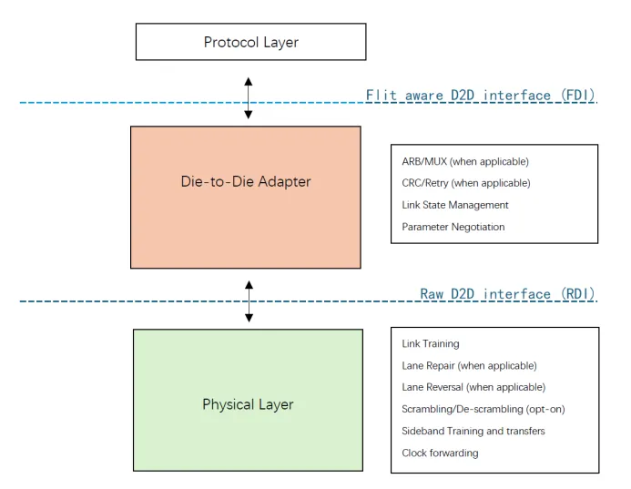
1. Layered Protocol ArchitectureUCIe utilizes a modular, layered architecture consisting of the PHY Layer, Adapter Layer, and Protocol Layer.
UCIe接口架构示意图
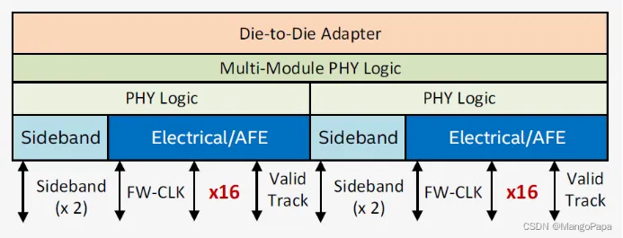
· PHY Layer: Handles physical signal transmission. It supports both Standard and Advanced Packaging, with per-lane rates ranging from 4 to 32 GT/s. It manages link training, lane reordering, and repair.
Two module configuration for standard package
(图源:【UCIe】初识 UCIe-CSDN博客)
· Adapter Layer: Ensures reliability through CRC (Cyclic Redundancy Check) and FEC (Forward Error Correction). It uses sideband messages to negotiate parameters with the connected die.
UCIe 与Adapter的连接
(图源:【UCIe】初识 UCIe-CSDN博客)
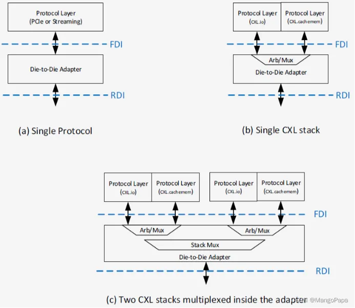
· Protocol Layer: Supports PCIe 6.0, CXL 2.0/3.0, and a "Streaming Protocol" for custom user-defined data.

UCIe Protocol层对应接口运行机制
2. Data Transmission Mechanisms
Mainband: Uses DDR (Double Data Rate) dual-edge sampling for high-speed traffic data.
Sideband: Acts as a back channel for link training, management, and register access, ensuring the Mainband is optimized for maximum throughput.
3. Link TrainingThrough a coordinated Link State Machine (LSM) across the layers, UCIe devices establish stable connections, negotiating speed and encoding parameters to ensure error-free communication.
III. UCIe and the Chiplet Ecosystem
Before UCIe, Chiplet adoption was hindered by proprietary interfaces. UCIe fills this gap by defining a universal software stack and physical layer specifications.
Key advantages of UCIe include:
Performance: High bandwidth density and ultra-low latency.
Reliability: Extremely low Bit Error Rates (BER < 1e-27 at low speeds; < 1e-15 at high speeds).
Scalability: Industry-wide support from giants like NVIDIA ensures a robust ecosystem for data centers and AI computing.
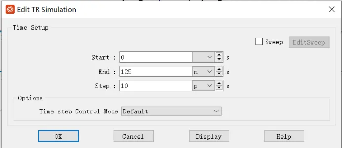
IV. Simulation and Verification with SIDesigner
Implementing UCIe presents significant Physical Layer (PHY) challenges. With lane rates hitting 32Gbps and dense signal routing in advanced packages, designers face severe Signal Integrity (SI) and Power Integrity (PI) risks.
Challenges in Chiplet Simulation:
Cross-Domain Effects: Combining SerDes-like high speeds with DDR-like parallel bus architectures.
Accuracy Requirements: Simulating ultra-low BER (1e-27) demands high-precision models (IBIS-AMI and S-Parameters).
System-Level Coupling: Addressing crosstalk, skew, and thermal-electrical effects in 2.5D/3D packages.
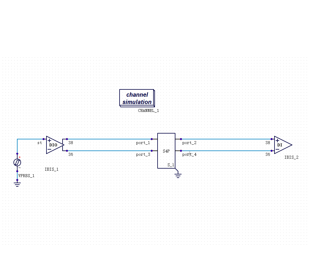
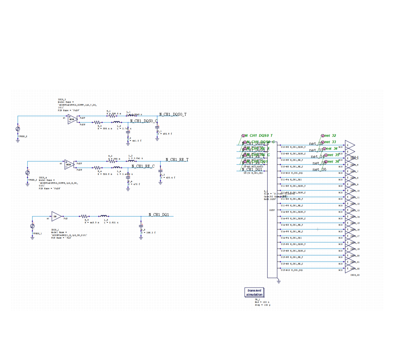
Using SIDesigner, engineers can construct accurate UCIe simulation circuits to validate link performance.
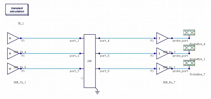
Simulation Setup Example:
Data Rate: 16Gbps (NRZ Modulation).
Method: Transient simulation with eye diagram overlay (~1500 UI).
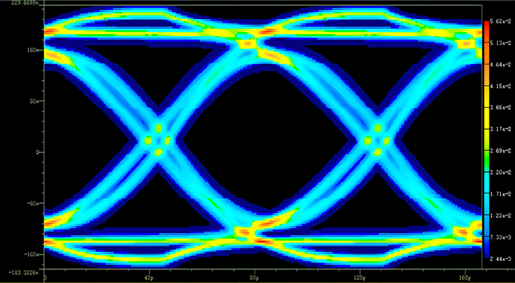
The results of the eye diagram simulation are as follows:
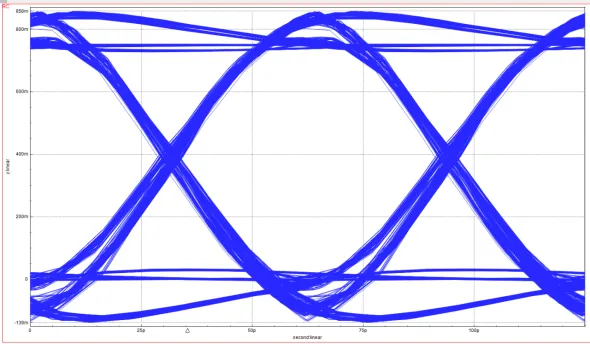
By analyzing the resulting Eye Diagram, engineers can visually assess whether the signal meets the physical constraints of speed and reliability, identifying specific issues like jitter or crosstalk to provide a precise basis for design optimization.
Visit our website to apply for a software trial of SIDesigner. For technical inquiries, please contact our support team to discuss how we can accelerate your high-speed interconnect designs!


Recommended
-
 Optimizing DDR Signal Integrity: Using DFQ Sensitivity Analysis (S1/ST) to Identify High-Leverage Design Variables
 2026.06.10
 -
 Efficiency Bottleneck in DDR5 Multi-Corner Timing Verification: PDA Analysis Methods
2026.05.27
Efficiency Bottleneck in DDR5 Multi-Corner Timing Verification: PDA Analysis Methods
2026.05.27 -
 The Mass Production Yield Trap After DDR5 SI Sign-off: Using DFQ to Predict Defect Rates Early
2026.05.07
The Mass Production Yield Trap After DDR5 SI Sign-off: Using DFQ to Predict Defect Rates Early
2026.05.07 -
 Selecting SI Simulation Tools: Practical Verification of SIDesigner's 4 Core Capabilities
2026.04.29
Selecting SI Simulation Tools: Practical Verification of SIDesigner's 4 Core Capabilities
2026.04.29