


Power Noise: Navigating the "Hidden Reefs" of Electronic Systems and Mitigation Strategies
-
 2025.07.28
In the vast and complex ocean of electronic systems, power noise acts like hidden reefs, silently threatening the stable operation of the system. From precision consumer electronics to massive industrial control systems, the impact of power noise is omnipresent. This article delves into the nature and hazards of power noise and explores mitigation strategies based on practical circuit models to build a solid foundation for reliable electronic design.
I. The Nature and Sources of Power Noise
1. The Physical Essence of Power Noise
Power noise manifests as non-ideal fluctuations in supply voltage or current, including ripple, spikes, and random noise.
· Ripple: Periodic low-frequency fluctuations originating from the energy storage and release characteristics during power conversion.
· Spikes: Transient high-frequency interference triggered by rapid switching actions or sudden load changes.
· Random Noise: Wideband spectral interference related to the thermal motion of electrons and the inherent characteristics of semiconductor devices.
These noises pull the power supply away from its ideal stable output, challenging any electronic circuit that relies on a steady voltage.
2. Sources of Noise in Circuit Models
Power noise is generated across multiple stages of the system:
· The Power Source: Despite nominal stability, insufficient filtering, inherent noise in linear regulators, or the Pulse Width Modulation (PWM) mechanism in switching power supplies can introduce foundational ripple.
· Voltage Regulator Modules (VRM): When a VRM dynamically adjusts output voltage to match load demands, the high-frequency toggling of switching transistors creates a significant rate of current change ($di/dt$). This rapid change induces voltage spikes across parasitic inductances (such as PCB traces or component leads) according to the formula:

· Packaging and Interconnect Parasitics: BGA solder balls, chip bumps, and PCB traces possess parasitic inductance and capacitance. These parameters can resonate with other circuit elements, amplifying low-frequency ripples and high-frequency spikes into wide-spectrum interference.
II. The Hazards of Power Noise
1. Degradation of Signal Integrity (SI)
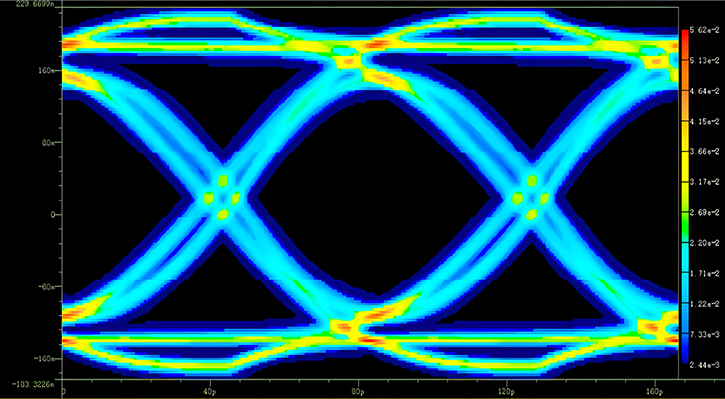
In high-speed digital circuits, power noise is a primary enemy of signal integrity. When noise amplitude exceeds a certain threshold—often just a few millivolts—the eye diagram of high-speed serial links (like DDR memory interfaces) significantly deteriorates.
Reduced Eye Height: Smaller noise margins lead to a higher risk of logic misinterpretation.
Narrowed Eye Width: Insufficient timing margins increase the probability of data sampling errors.
Ultimately, this leads to a spike in the Bit Error Rate (BER), compromising the accuracy of data transmission.
2. Reduced Device Longevity and Reliability
Long-term exposure to power noise erodes the reliability of electronic components.
Thermal Cycling: Power devices (like MOSFETs in a VRM) experience frequent thermal cycling due to noise-induced current fluctuations, leading to material fatigue and premature failure.
Passive Component Stress: High-frequency noise components increase the loss in Equivalent Series Resistance (ESR) of capacitors, causing them to overheat and shortening their lifespan.
III. Mitigation Strategies for Power Noise
1. Management of Parasitic Parameters
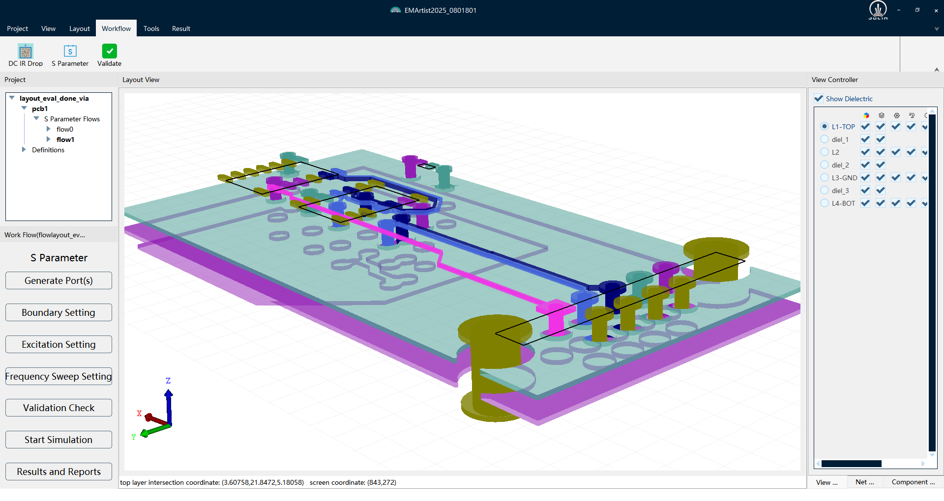
Optimizing BGA solder ball layouts to reduce spacing can effectively lower parasitic inductance. Utilizing packaging materials with low ESR and low ESL (Equivalent Series Inductance) minimizes the amplification of noise. Precise electromagnetic (EM) simulation is essential to blocking noise propagation at the physical level.
2. Local Decoupling Networks
Deploying local decoupling capacitors near chip pins or critical circuit nodes creates a "charge reservoir." These capacitors provide instantaneous charge when the load requires a sudden burst of current, suppressing voltage fluctuations.
Example: Configuring a combination of small-capacity decoupling capacitors (e.g., 10nF + 100nF) next to BGA pins allows the system to respond to load changes within nanoseconds.
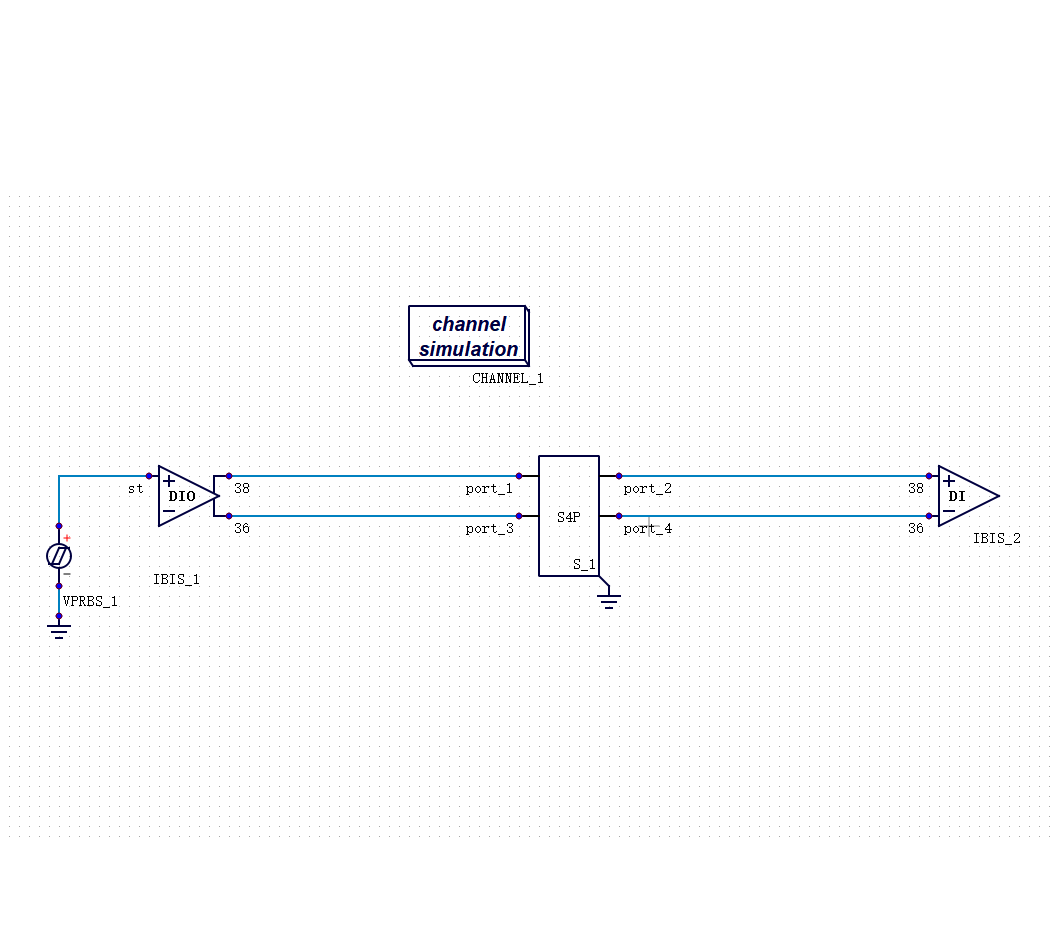
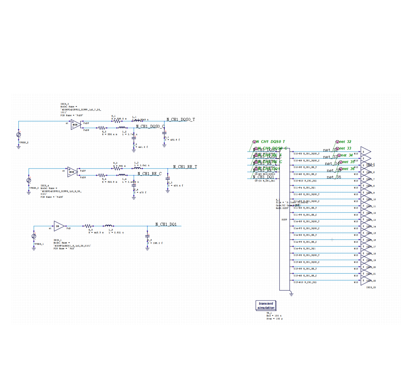
IV. Simulation with SIDesigner
Using the SIDesigner simulation platform developed by Julin Technology, engineers can construct sophisticated simulation circuits to analyze power noise.
Key Benefits of SIDesigner Simulation:
· Comprehensive Assessment: Evaluate system performance under various noise scenarios.
· Optimization: Improve system reliability and stability before physical prototyping.
· Acceleration: Speed up the R&D and iteration process by identifying "hidden reefs" early in the design phase.
Conclusion
Power noise is an unavoidable challenge, but its hazards are not invincible. By understanding its origins and utilizing advanced EDA tools like SIDesigner for all-around optimization—from power topology to packaging—designers can ensure the signal integrity and long-term reliability of modern electronic systems.


Recommended
-
 Optimizing DDR Signal Integrity: Using DFQ Sensitivity Analysis (S1/ST) to Identify High-Leverage Design Variables
 2026.06.10
 -
 Efficiency Bottleneck in DDR5 Multi-Corner Timing Verification: PDA Analysis Methods
2026.05.27
Efficiency Bottleneck in DDR5 Multi-Corner Timing Verification: PDA Analysis Methods
2026.05.27 -
 The Mass Production Yield Trap After DDR5 SI Sign-off: Using DFQ to Predict Defect Rates Early
2026.05.07
The Mass Production Yield Trap After DDR5 SI Sign-off: Using DFQ to Predict Defect Rates Early
2026.05.07 -
 Selecting SI Simulation Tools: Practical Verification of SIDesigner's 4 Core Capabilities
2026.04.29
Selecting SI Simulation Tools: Practical Verification of SIDesigner's 4 Core Capabilities
2026.04.29